Circuit arrangement for rapidly controlling in particular inductive loads

a technology of inductive load and circuit arrangement, which is applied in the direction of electronic switching, pulse technique, semiconductor devices, etc., can solve the problems of only becoming economically viable, and only becoming conducting between drain and source of n-channel transistors, etc., and achieves the effect of rapid switching on and o

Inactive Publication Date: 2006-03-28
SIEMENS AG
View PDF37 Cites 4 Cited by
  • Summary
  • Abstract
  • Description
  • Claims
  • Application Information

AI Technical Summary

Benefits of technology

[0010]The object of the present invention is to provide a circuit arrangement overcoming the stated problems of the prior art, in particular specifying an inexpensive arrangement which can be implemented without complex circuitry and which allows a high-side switch implemented as an N-channel MOS power transistor to be rapidly switched on and off. It is another object of the present invention to further develop a generic circuit arrangement in such a way that the switching times of the MOS power transistor are adjustable over a wide range.
[0017]The invention is based on the generic circuit arrangement according to FIG. 2 in that the switching-means transistor is connected as a power source. Through this measure, the invention overcomes the dependence on current densities which are supplied by a constant voltage source as a function of the network parameters. The required current density rather becomes an adjustable quantity with adaptable output voltage of the current source. As the current density is the actual critical variable for driving switching transistors, the present invention provides the basis for more precise adjustability of the switching processes than has been possible with the prior art.
[0018]In an advantageous development of the present invention, the first switching-means transistor connected as a current source, preferably a pnp transistor, is part of a current mirror circuit. Although there are different possibilities for implementing a current source using a transistor, the current mirror circuit is particularly favorable, as it enables the current density of the output current to be adjusted particularly easily and over a wide range, which means direct adjustability of the switching times of the MOS power transistor.
[0020]In a preferred development of the circuit arrangement according to the invention, it is provided that the collector current of the first switching-means transistor flows to the gate electrode of the switching transistor via a diode connected in the flow direction. As a result, once the gate capacitor has been charged, the charge stored there cannot drain away elsewhere, which means that the switching transistor can remain turned on for longer.
[0023]In addition, the current mirror circuit advantageously incorporates a diode connected in series with the first current mirror resistor and in the flow direction of the current mirror input current. This is implemented in such a way that it prevents current flow from the base to the emitter of the first switching-means transistor, but permits a current mirror circuit input current from the low voltage source to ground in the conducting state.

Problems solved by technology

Attempts are therefore being made to implement even high-side switches with N-channel transistors, the main problem being that an N-channel transistor only becomes conducting between drain and source in the event of a positive gate voltage.
Although this principle enables high voltages to be generated in a simple and cost-effective manner, the current handling capacity of a voltage source produced in this way using a charge pump is mostly low.
Because of the auxiliary voltage source required, which is raised above the supply potential and can therefore only be used for the explained purpose, the circuit described is expensive and only becomes economically viable when used for a plurality of high-side switches.
The disadvantage, however, is that the current decays relatively quickly even with a high-value capacitor, so that lasting turn-on of the MOS power transistor is not possible with this circuit.
The main disadvantage of the circuit arrangements according to the prior art is that the switching edges, i.e. basically the switching rate, is only adjustable to a very limited extent.
This is disadvantageous because, for fast switching processes, a balanced compromise must always be found between excessively slow switching on the one hand, resulting in heating of the transistors and therefore increased switching losses, and excessively rapid switching on the other, resulting in an increased electromagnetic interference level.

Method used


Image

  • Circuit arrangement for rapidly controlling in particular inductive loads
  • Circuit arrangement for rapidly controlling in particular inductive loads
  • Circuit arrangement for rapidly controlling in particular inductive loads

Examples


Embodiment Construction

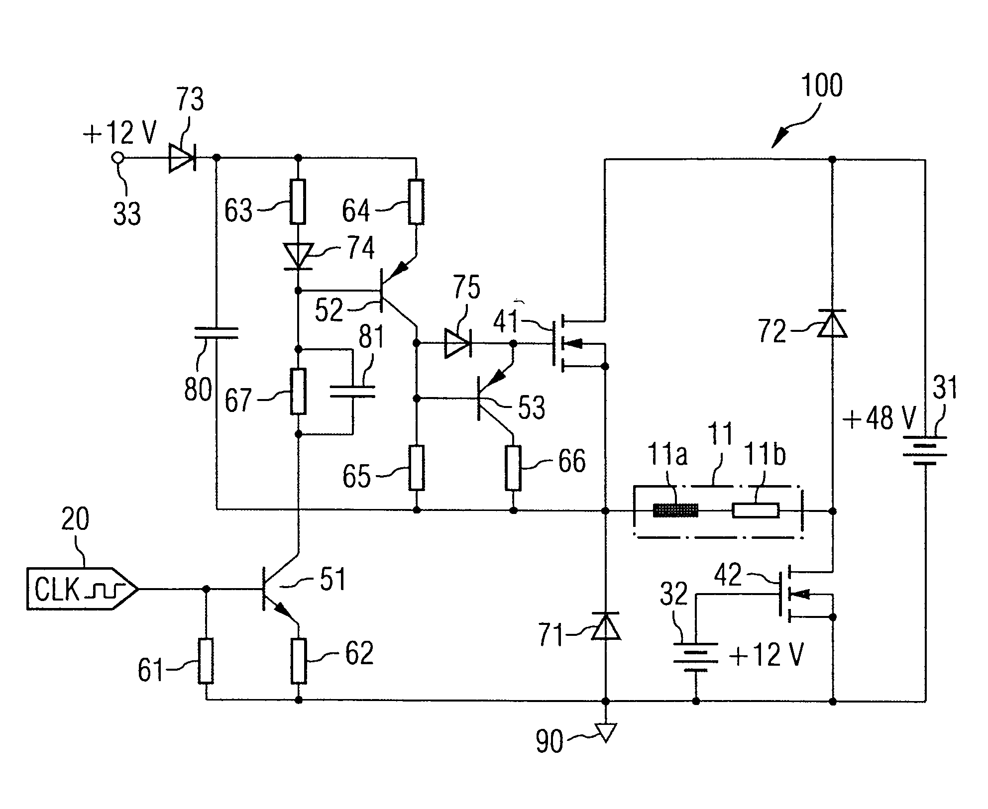
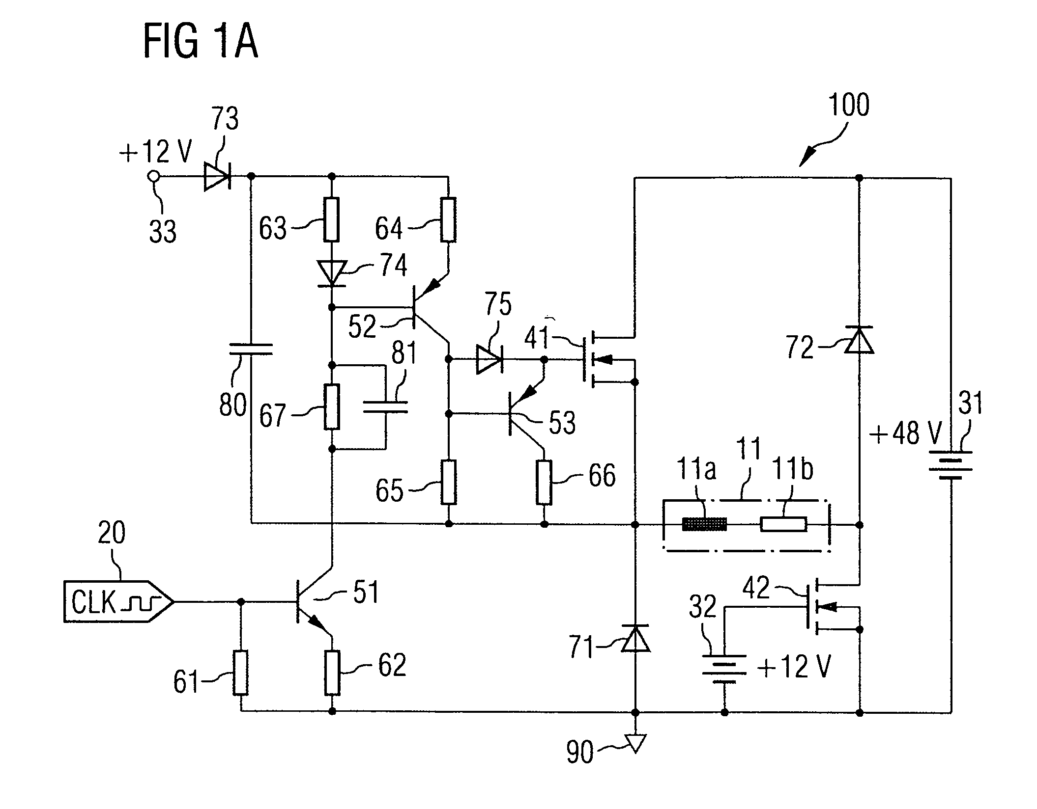
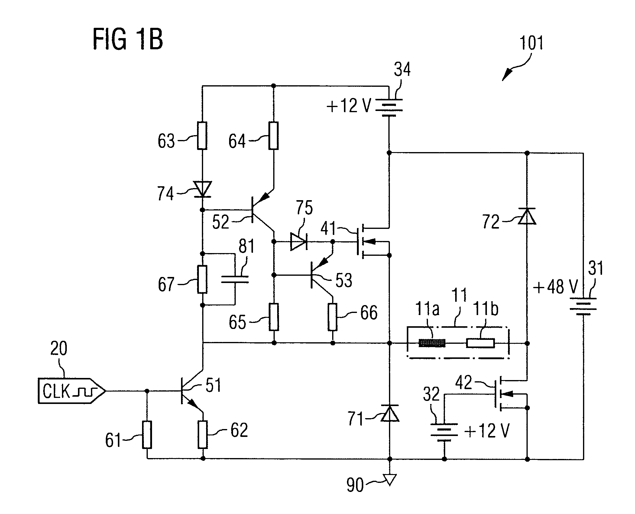
[0034]FIG. 1a illustrates a circuit arrangement 100 according to a particularly preferred exemplary embodiment of the invention for driving an electromagnetic injection valve 11, depicted as a series circuit comprising the actual coil inductor 11a, e.g. 150 μH of the electromagnet and the winding resistor 11b, e.g. 0.5 Ω. The valve 11 can be loaded by a voltage supply 31 with a voltage of e.g. 48 V clocked by a control signal 20 implemented as a square-wave voltage, said signal advantageously originating from a microcontroller (not shown). The switching transistor 41 implemented as an N-channel MOS power transistor and connected on the high side is used as the switch. The control clock is injected into the network via switching means incorporating a switching-means transistor 51. The circuit arrangement is part of an extended drive of 16 valves in an internal combustion engine. The valve 11 is selected via a selecting transistor 42, preferably likewise a MOS power transistor, implem...


PUM


Abstract

A circuit arrangement for rapidly switching in particular inductive loads, comprises a load (11) being connectable to a supply voltage source (31) by means of a switching transistor(41) implemented as an N-channel MOS power transistor and connected as a high-side switch, a potential exceeding the voltage of the supply voltage source (31) being applicable to the gate electrode of the switching transistor (41) by controllable switching means, said switching means incorporating at least a first switching-means transistor (52) whose collector current can flow at least in part to the gate electrode of the switching transistor (41) during the conducting state. The first switching-means transistor (52) is connected as a current source. Furthermore, the first switching-means transistor (52) connected as a voltage source can be part of a current mirror circuit.

Description

PRIORITY[0001]This application claims foreign priority of the German application DE 10252827.6 filed on Nov. 13, 2002.TECHNICAL FIELD OF THE INVENTION[0002]The invention relates to a circuit arrangement for rapidly switching in particular inductive loads, a load being connectable to a supply voltage source by means of a switching transistor implemented as an N-channel MOS power transistor and connected as a high-side switch, a potential exceeding the voltage of the supply voltage source being applicable to the gate electrode of said switching transistor by controllable switching means and said switching means incorporating at least one first switching-means transistor whose collector current can flow at least in part to the gate electrode of the switching transistor in the conducting state.BACKGROUND OF THE INVENTION[0003]Circuit arrangements of this kind are used, for example, in automotive electronics where the operation of fast-switching, inductive loads by means of MOS power tra...

Claims


Application Information

Patent Timeline
Patent Type & Authority Patents(United States)
IPC IPC(8): H03K17/14H03K17/0412H03K17/06
CPCH03K17/063H03K17/04123
Inventor BOLZ, STEPHANLUGERT, GUNTER
Owner SIEMENS AG
Why Eureka
Try Eureka