
Static random access memory and semiconductor device using MOS transistors having channel region electrically connected with gate

a random access memory and gate technology, applied in transistors, solid-state devices, instruments, etc., can solve the problems of reduced operating speed, increased power consumption, increased cost, etc., and achieve high electrostatic withstand voltage and high reliability of semiconductors

Inactive Publication Date: 2006-03-28
SHARP KK
View PDF13 Cites 4 Cited by
  • Summary
  • Abstract
  • Description
  • Claims
  • Application Information

AI Technical Summary

Benefits of technology

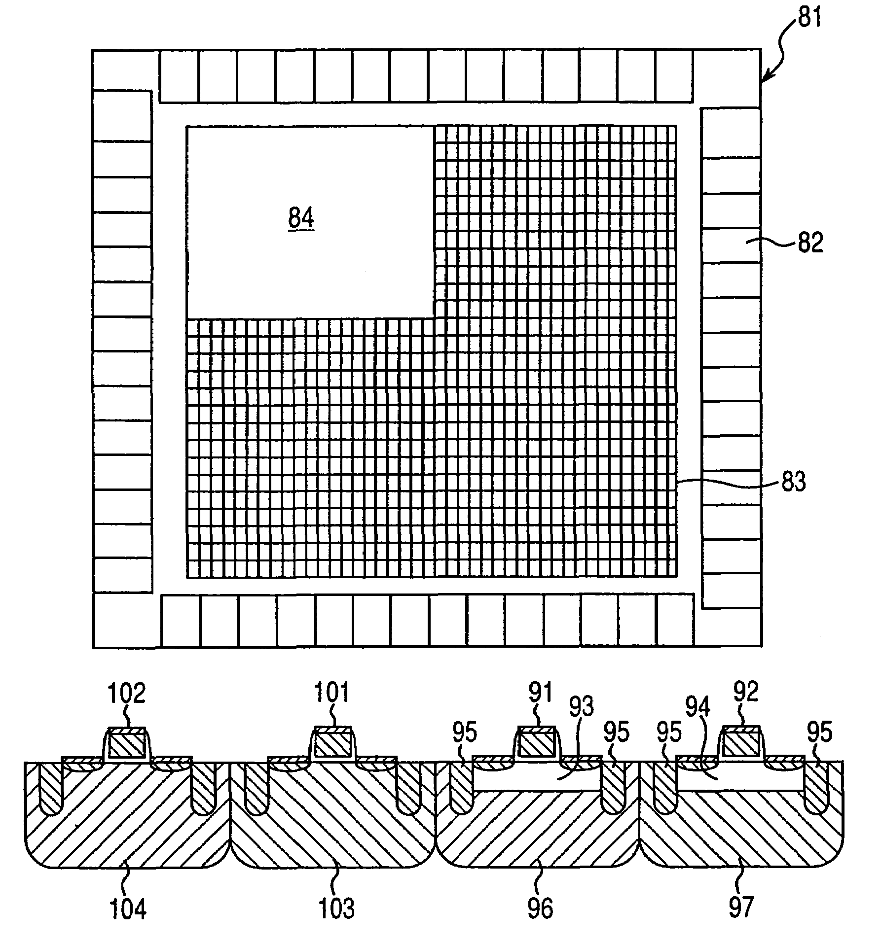
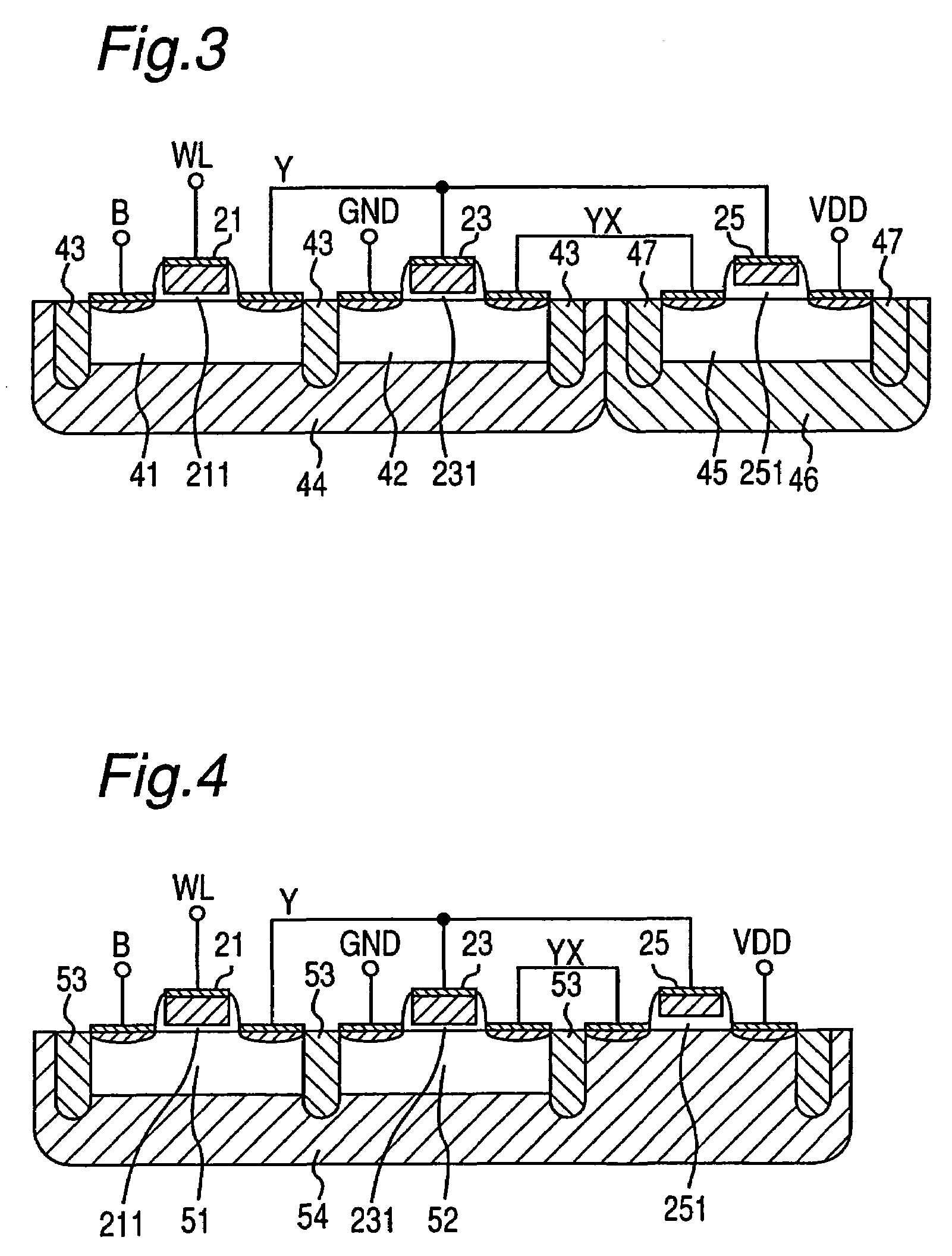
[0013]The MOS transistor whose gate is electrically connected with the channel-forming semiconductor region is referred to as “DTMOS (Dynamic Threshold MOS) transistor” or simply “DTMOS” herein. Because the gate is electrically connected with the channel-forming semiconductor region in the DTMOS transistors, each MOS transistor is controllable to have a low threshold voltage |Vth| in its ON stage and a high threshold voltage |Vth| in its OFF stage. This enables a low-voltage operation at 0.5 V and prevents leak current in the OFF stage from increasing. Thus, the SRAM of the present invention is allowed to consume less power than the conventional SRAM. Furthermore, because |Vth| of the DTMOS in the ON stage is low, the ON-state resistance is also small, and it is possible to increase the writing / reading speed. If the writing / reading speed for the DTMOS is maintained equivalent to the conventional speed, then it is possible to narrow the gate width to the extent according to a decrease of the ON-state resistance to thereby achieve the reduction in area of the SRAM.
[0015]According to the above construction, the N-type MOS transistors included in the memory cells or SRAM cells are DTMOS transistors. This allows the low-voltage operation, low consumption of power and high writing / reading speed of the SRAM cells. If the writing / reading speed is maintained equivalent to the conventional speed, then the reduction in area of the SRAM cells is achieved.
[0017]In this case, because the ON-state resistance of the P-type MOS transistors increases, the current decreases, allowing the NMOS transistors to be constructed in a smaller size. Therefore, it is possible to achieve a further reduction in area, a small leak current and a low consumption of power of the SRAM cells.
[0022]As described above, the DTMOS transistors have a low ON-state resistance and are able to suppress the leak current in the OFF stage. Therefore, the lower voltage operation, lower consumption of power, higher writing speed and size reduction of the write circuit are achieved.
[0024]In this case, at the time of writing to the memory cells, the high-level potentials of the bit line and the inverted bit line are reduced. Thus, a further reduction in consumption of power is achieved.

Problems solved by technology

That is, generally, the consumption of power increases when an LSI is operated at high speed.
Therefore, in order to stably operate the LSI, a ceramic package and radiator fins and so on are needed, resulting in an increased cost.
However, the above conventional SRAM has the following problems.
However, if the voltage VDD is lowered, then the driving current of the MOS transistors becomes so small that delay time of the circuit disadvantageously increases, resulting in the reduction of the operating speed.
However, if the threshold voltage Vth is reduced, then a leak current of the MOS transistor increases, and this leads to the problem that the power consumption increases great due to the existence of the leak current even in a standby mode.

Method used


Image

  • Static random access memory and semiconductor device using MOS transistors having channel region electrically connected with gate
  • Static random access memory and semiconductor device using MOS transistors having channel region electrically connected with gate
  • Static random access memory and semiconductor device using MOS transistors having channel region electrically connected with gate

Examples


Embodiment Construction

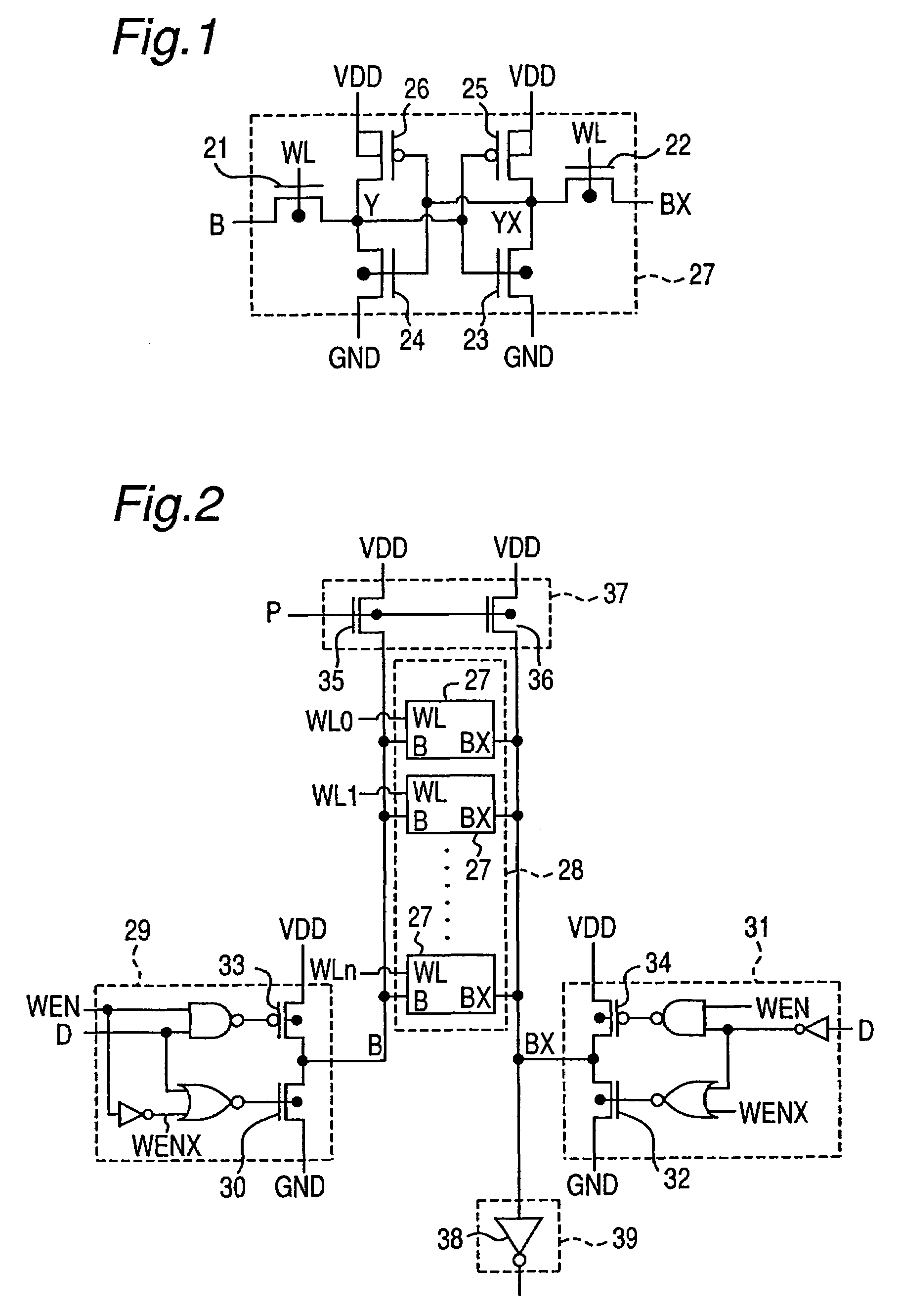
[0040]The present invention will be described in detail below on the basis of the embodiments shown in the drawings. FIG. 1 is a circuit diagram showing an example of SRAM cells of the SRAM according to the present embodiment. The SRAM cell 27 in the present embodiment is also constructed of two PMOS transistors and four NMOS transistors.

[0041]A bit line B is connected to the source (drain) of a first NMOS transistor 21. A word line WL is connected to the gates of the first NMOS transistor 21 and a second NMOS transistor 22. An inverted bit line BX is connected to the source (drain) of the second NMOS transistor 22.

[0042]The drain (source) Y that belongs to the first NMOS transistor 21 and is not connected to the bit line B is connected to the gates of a third NMOS transistor 23 and a first PMOS transistor 25 and further connected to the drains of a fourth NMOS transistor 24 and a second PMOS transistor 26.

[0043]The drain (source) XY that belongs to the second NMOS transistor 22 and...


PUM


Abstract

In an SRAM, memory cells are each constructed of four NMOS transistors and two PMOS transistors 25 and 26. The four NMOS transistors are each constructed of DTMOS in which the channel region is electrically connected to the gate. In each NMOS transistor, a threshold voltage Vth is lower in an ON stage than in an OFF stage. The threshold voltage Vth in the OFF stage is equivalent to that of an ordinary NMOS transistor in which the channel region is not electrically connected to the gate. Read and write circuits of the SRAM also include MOS transistors formed of DTMOS in which the channel region is electrically connected to the gate.

Description

[0001]This application is a continuation of Ser. No. 09 / 412,328 filed Oct. 5, 1999, now U.S. Pat. No. 6,724,065.BACKGROUND OF THE INVENTION[0002]The present invention relates to a static random access memory (“SRAM” hereinafter) and a semiconductor device.[0003]By virtue of the progress of microfabrication technology, the operation speed and the integration degree of LSIs (Large Scale Integrated Circuits) have been increasing in recent years. In order to put an LSI that operates at high speed into practical use, the reduction in consumption of power of the LSI is one of important technical requirements. That is, generally, the consumption of power increases when an LSI is operated at high speed. Therefore, in order to stably operate the LSI, a ceramic package and radiator fins and so on are needed, resulting in an increased cost. In recent years portable devices have been advancing toward further reduction in size and weight, and the reduction in consumption of power is important al...

Claims


Application Information

Patent Timeline
IPC IPC(8): H01L29/76H01L29/94H01L31/062H01L31/113H01L31/119G11C11/413G11C11/412H01L21/8244H01L27/11H01L29/78
CPCG11C11/412H01L27/1104Y10S257/903H10B10/12G11C11/413
Inventor SATO, YUICHI
Owner SHARP KK
Learn More