
Post treatment of low k dielectric films

a low-k dielectric constant and film technology, applied in the manufacturing of basic electric elements, electric devices, semiconductor/solid-state devices, etc., can solve problems such as mechanical strength and failure of integrated circuits

Active Publication Date: 2006-03-28
APPLIED MATERIALS INC
View PDF36 Cites 523 Cited by
  • Summary
  • Abstract
  • Description
  • Claims
  • Application Information

AI Technical Summary

Benefits of technology

The invention provides a method for processing a substrate by depositing a low dielectric constant film and then heating it to a desired temperature and cooling it quickly. The film can be heated and cooled within a time period of 0.5 to 5 minutes. The method can also involve treating the film with electron beam or UV radiation treatment. The technical effect of this invention is to provide a method for creating high-quality low dielectric constant films with improved properties such as low dielectric constant, low resistivity, and high thermal stability.

Problems solved by technology

One challenge in this area has been to develop a Si, C, and O containing film that has a low k value and also exhibits desirable thermal and mechanical properties.
Often Si, C, and O containing films that have a desirable dielectric constant exhibit poor mechanical strength and are easily damaged by etch chemistry and plasma exposure during subsequent processing, causing failure of the integrated circuit.

Method used


Image

  • Post treatment of low k dielectric films
  • Post treatment of low k dielectric films
  • Post treatment of low k dielectric films

Examples


example 1

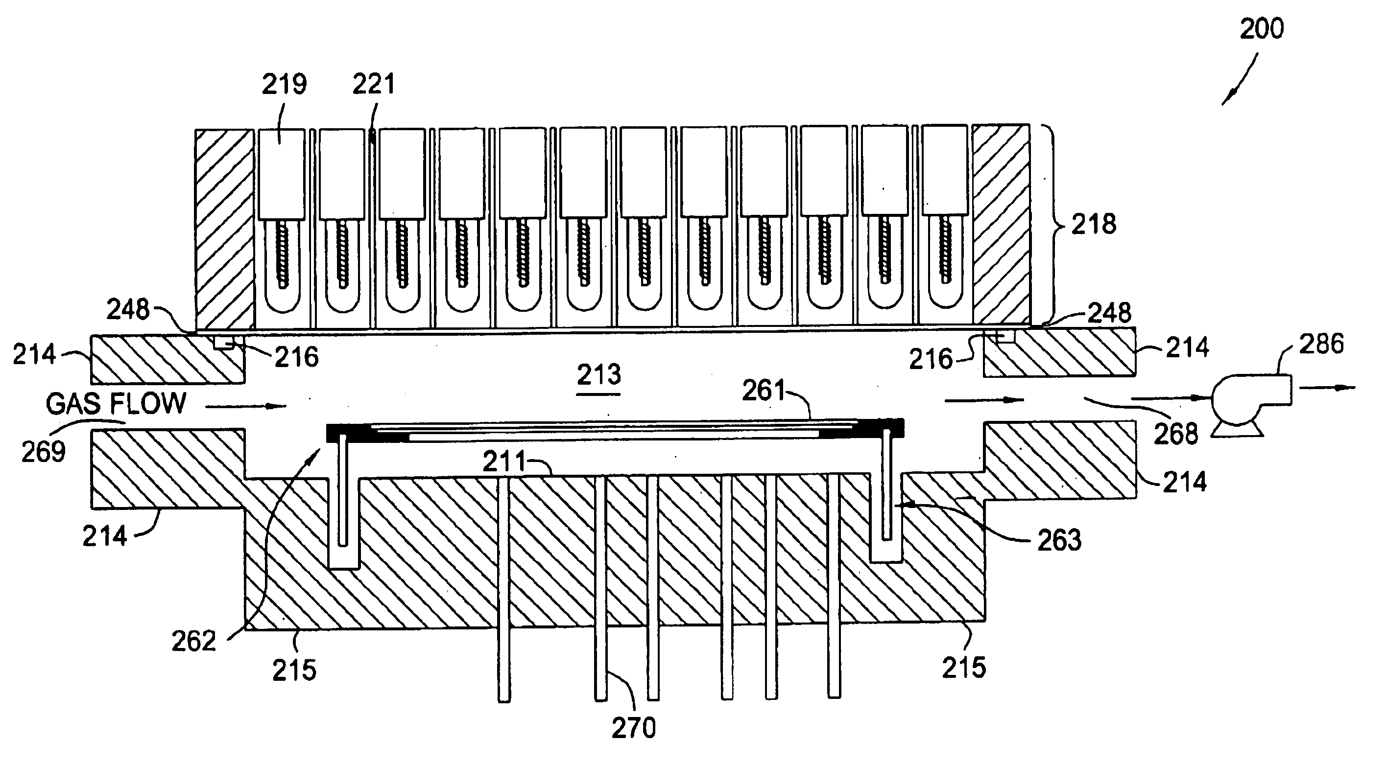
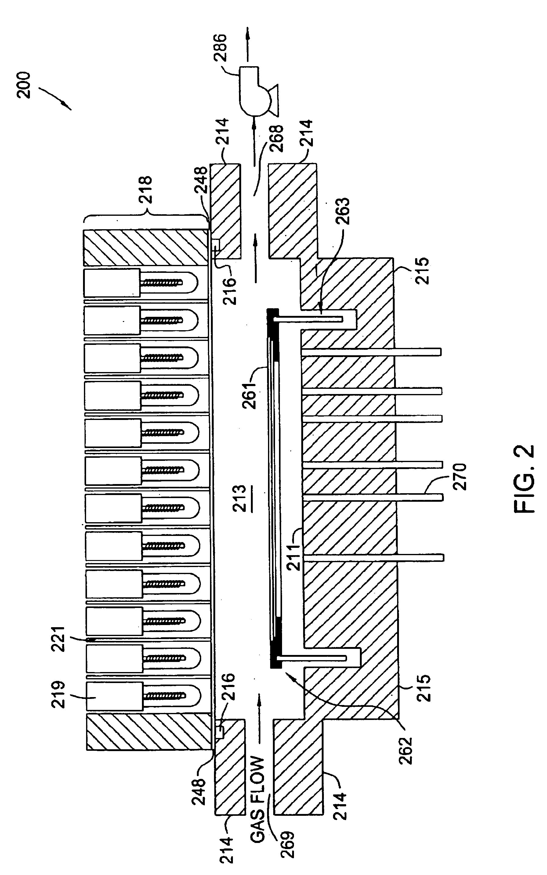
[0062]A low dielectric constant film was deposited on a substrate as described in Comparison Example 1. The low dielectric constant film was post-treated in a Radiance™ RTP chamber by rapidly heating the dielectric constant film from room temperature to a temperature of 800° C. and then immediately cooling the low dielectric constant film to a temperature of 120° C. such that the film is heated and cooled within 30 seconds. As deposited, the low dielectric constant film had a thickness of 5,036 Å. After the post-treatment, the low dielectric constant film had a thickness of 5,021 Å (shrinkage of 0.3%). After the post-treatment, the low dielectric constant film had a dielectric constant (k) of 2.53, and a hardness of 0.62 gPa.

example 2

[0063]A low dielectric constant film was deposited on a substrate as described in Comparison Example 1. The low dielectric constant film was post-treated in a Radiance™ RTP chamber by rapidly heating the dielectric constant film from room temperature to a temperature of 800° C. and then immediately cooling the low dielectric constant film to a temperature of 120° C. such that the film is heated and cooled within 30 seconds. As deposited, the low dielectric constant film had a thickness of 5,011 Å. After the post-treatment, the low dielectric constant film had a thickness of 4,996 Å (shrinkage of 0.3%). After the post-treatment, the low dielectric constant film had a dielectric constant (k) of 2.44.

[0064]Examples 1 and 2 show that post-treating low dielectric constant films by rapidly heating and cooling the low dielectric constant films according to embodiments described herein resulted in films having a lower dielectric constant than films that were not post-treated or films that w...


PUM

PropertyMeasurementUnit
temperatureaaaaaaaaaa

Abstract

A method of depositing a low dielectric constant film on a substrate and post-treating the low dielectric constant film is provided. The post-treatment includes rapidly heating the low dielectric constant film to a desired high temperature and then rapidly cooling the low dielectric constant film such that the low dielectric constant film is exposed to the desired high temperature for about five seconds or less. In one aspect, the post-treatment also includes exposing the low dielectric constant film to an electron beam treatment and / or UV radiation.

Description

BACKGROUND OF THE INVENTION[0001]1. Field of the Invention[0002]Embodiments of the present invention relate to the fabrication of integrated circuits. More particularly, embodiments of the present invention relate to a process for depositing and post-treating low dielectric constant films.[0003]2. Description of the Related Art[0004]Semiconductor device geometries have dramatically decreased in size since such devices were first introduced several decades ago. Since then, integrated circuits have generally followed the two year / half-size rule (often called Moore's Law), which means that the number of devices that will fit on a chip doubles every two years. Today's fabrication plants are routinely producing devices having 0.13 μm and even 0.1 μm feature sizes, and tomorrow's plants soon will be producing devices having even smaller geometries.[0005]In order to further reduce the size of devices on integrated circuits, it has become necessary to use conductive materials having low res...

Claims


Application Information

Patent Timeline
Patent Type & Authority Patents(United States)
IPC IPC(8): H01L21/31H01L21/461H01L21/314H01L21/316
CPCH01L21/02126H01L21/02216H01L21/31633H01L21/02348H01L21/02351H01L21/02274H01L21/02203
Inventor CUI, ZHENJIANGCHANG, JOSEPHINE J.DEMOS, ALEXANDROS T.ARGHAVANI, REZAWITTY, DEREK R.ARMER, HELEN R.DIXIT, GIRISH A.M'SAAD, HICHEM
Owner APPLIED MATERIALS INC
Learn More