Integrated high-speed multiple-rate optical-time-division-multiplexing module

a technology of optical time division and multi-channel, applied in multiplex communication, instruments, optical elements, etc., can solve the problems of high cost, high complexity, and inability to achieve higher rates per single optical channel, and achieve high-speed, difficult-to-reach targets, etc., to achieve the effect of reducing the electronic bandwidth bottleneck

Active Publication Date: 2006-03-07
MOLEX INC
View PDF3 Cites 13 Cited by
  • Summary
  • Abstract
  • Description
  • Claims
  • Application Information

AI Technical Summary

Benefits of technology

[0016]Optical time division multiplexing (OTDM) is a technique which takes advantage of the Return-to-Zero (RZ) transmission format to alleviate the electronic bandwidth bottleneck. In its simplest form, the OTDM technique attempts to insert one bit of data between two adjacent bits to produce a higher (e.g. double) data rate. Very extensive research has been performed within the field of optical time division multiplexing (OTDM) for generating ultra-high bit rate signals at and in excess of 40 Gbit / s. To generate OTDM signals, very nigh quality short pulse sources based on mode-locking lasers or external modulators are required, as well as high-precision optical multiplexers. The present invention proposes a novel optical time division multiplexing (OTDM) module capable of multiple-rate multiplexing. In the preferred embodiments, this multi-rate OTDM module is integrated on an optical chip. In so doing at least some of the problems related to optically multiplexing data streams of differing bit rates are mitigated by providing a single integrated multiple-rate OTDM module which can optically multiplex signals having different bit-rates. The present invention also provides for the integration of an optical pulse source chip and a multiple-rate OTDM chip onto a single substrate or platform using hybrid packaging technology. In so doing at least some of the problems mentioned above with respect to size, complexity, cost, and problems associated with optical connections of present solutions are mitigated.

Problems solved by technology

However, the operation and management of DWDM systems is highly complicated and costly.
Therefore, a key issue is to achieve higher rates per single optical channel which cannot be achieved by electrical time division multiplexing (ETDM) technology.
With known transmitter combinations of semiconductor lasers with external modulators, such target values are attainable only with great difficulty.
However, electrical components for ETDM technology such as electrical multiplexers and demultiplexers (EMUXs and EDMUXs), that can achieve the high data rates (e.g. work beyond 40 Gbit / s) required today, are not expected to be available for the next several years.
However, there are downsides to OTDM technology as well Specifically, current OTDM implementations are relatively more complicated, expensive, and inflexible than their counterpart ETDM solutions.
So even though it's easier to get to 40 Gbit / s systems using OTDM technology today (because 40 Gbit / s electronics have not been fully developed), these are not very easy systems to build and manage.
These kind of approaches are rather expensive and bulky and face stability and processing problems.
Moreover, these approaches are inflexible in that they inherently employ a fixed delay for a single expected data rate.
In situations where an expected data stream will vary in bit rate, or in which the OTDM is required to accommodate different signals with different bit-rates, current OTDM modules will not be capable of proper time domain multiplexing because the fixed optical delay utilized therein will not match that required for multiplexing data streams of the various bit rates.
Solutions based on this approach are bulky, complicated and expensive and may also suffer from signal loss associated with chip-to-chip connections.
Such an approach leads to many problems when connecting an optical pulse source to an OTDM module, such as difficulty in polarization matching, optical power loss, and optical reflection.
At a fiber-to-fiber connection between the waveguide from the pulse source and that of the OTDM module, a great optical power loss can be produced if the waveguide dimensions (e.g. fiber core dimensions), shapes, orientations, and physical positions are mismatched.

Method used


Image

  • Integrated high-speed multiple-rate optical-time-division-multiplexing module
  • Integrated high-speed multiple-rate optical-time-division-multiplexing module
  • Integrated high-speed multiple-rate optical-time-division-multiplexing module

Examples


Embodiment Construction

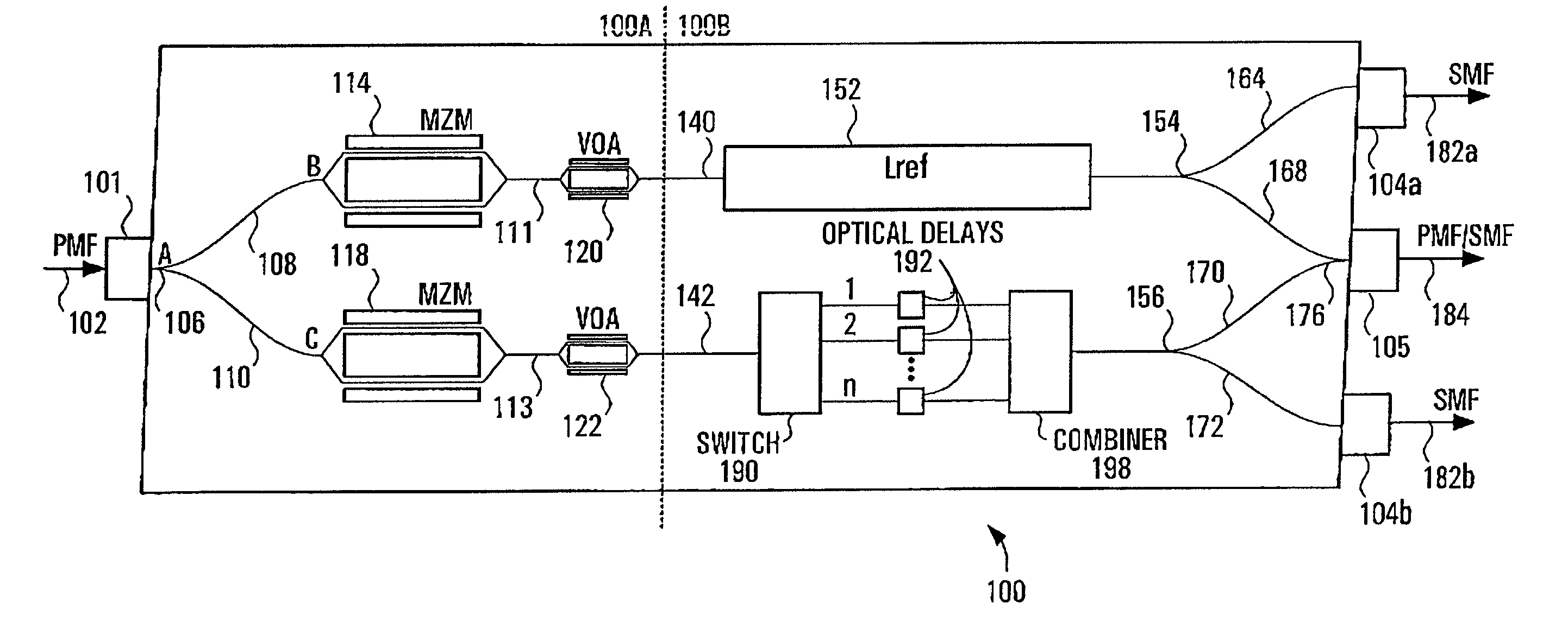
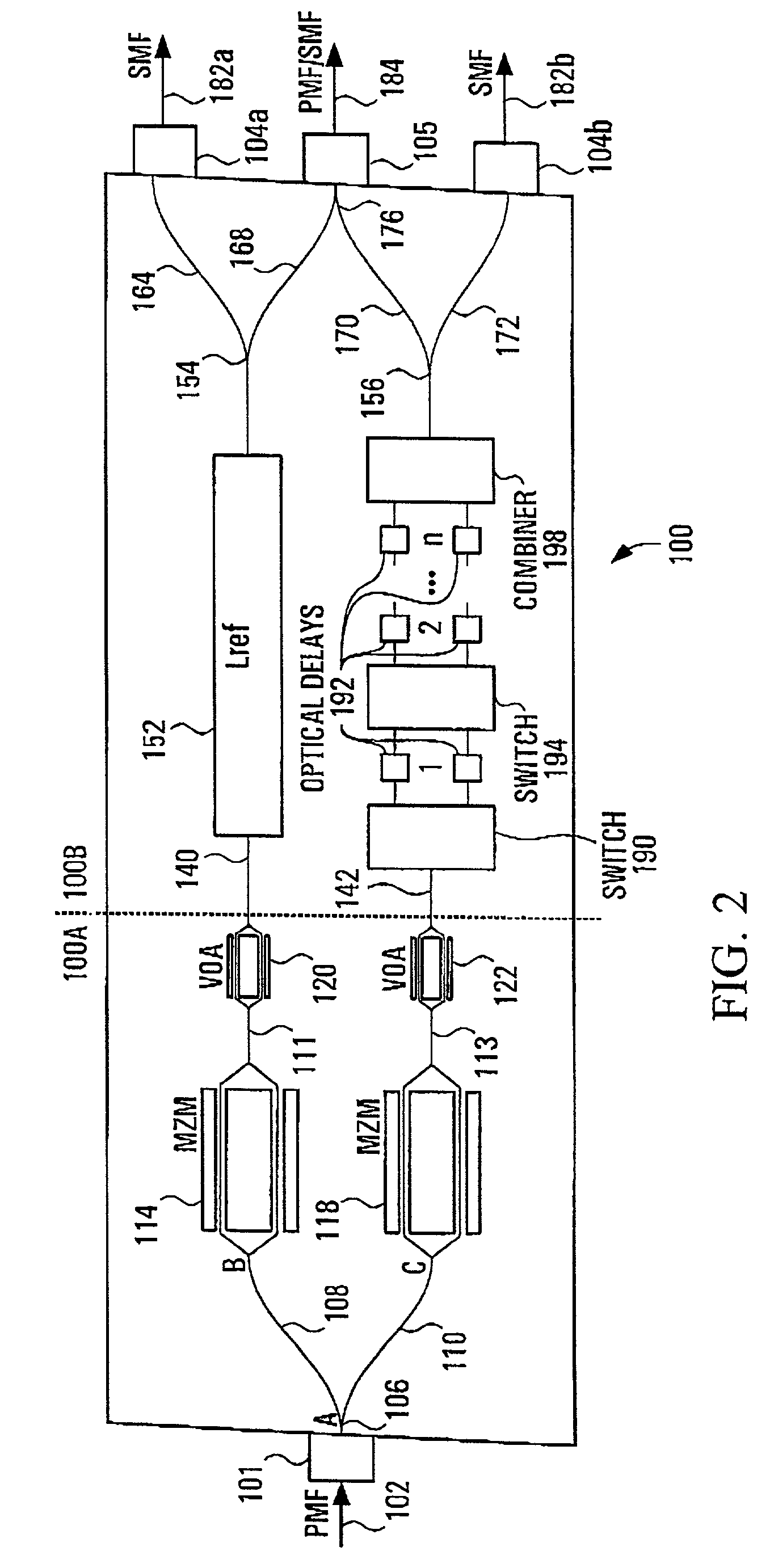
[0044]Referring to FIG. 1, an integrated high-speed multiple-rate OTDM module 100 constructed according to an embodiment of the invention utilizing an optical delay switching and combining array in a parallel configuration is described. For ease of description the multiple-rate OTDM module 100 will be discussed in terms of a twin-modulator portion 100A and a time-delay portion 100B, both described in more detail below.

[0045]A twin-modulator portion 100A of the multiple-rate OTDM module 100 receives an input signal (not shown) via an input polarization maintaining fiber (PMF) 102 having an end portion secured within a fiber tube 101. The waveguide structure of the twin-modulator portion 100A comprises a Y-branch junction 106 which divides the input signal delivered by the input PMF 102 among waveguide portions 108 and 110 denoted by paths AB and AC, respectively. The twin-modulation portion 100A of the multiple-rate OTDM module 100 comprises first and second Mach-Zehnder modulators 1...


PUM


Abstract

A novel integrated multiple-rate optical time division multiplexing (OTDM) module is disclosed. An integrated set of modulators generates optical RZ signal streams which are then time-delayed by a set of integrated optical delay switching and combining arrays and interleaved to produce an OTDM signal. The integrated optical delay switching and combining arrays are adapted to be controllably set to various delays to facilitate interleaving of many possible bit-rates. Such an approach alleviates stability problems offered by conventional fiber-based OTDM technology, increases flexibility, aids in reducing the size, complexity, and cost. Furthermore, the OTDM chip of the present invention offers fine tuning capabilities thereby allowing for slight adjustments in the interleaving of optical signal streams if needed. The present invention also provides for the integration of an optical pulse source chip and a multiple-rate OTDM chip onto a single substrate or platform using hybrid packaging technology.

Description

FIELD OF THE INVENTION[0001]This invention relates to optical time division multiplexing (OTDM) and more particularly to a multiple-rate optical time division multiplexing module integrated onto an optical chip, and a multiple-rate OTDM module integrated onto a single substrate having an optical pulse source (OPS).BACKGROUND OF THE INVENTION[0002]In general, there are two common data formats for the transmission of high-speed digital data. Non-Return-to-Zero (NRZ) signal format is the more popular of the two formats due to its inherent simplicity. In this particular format, each “0” or “1” data bit is represented by a low or high signal level, Respectively, lasting an entire clock period. However, with ever-increasing data rates, especially in optical transmission systems, Return-to-Zero (RZ) signal formats are becoming the transmission format of choice. In RZ modulation format, each data bit occupies only a portion of tile clock period creating a distinct transition between adjacen...

Claims


Application Information

Patent Timeline
Patent Type & Authority Patents(United States)
IPC IPC(8): H04J14/08
CPCH04J14/08
Inventor LEE, KU-SUENLI, JINGHUIWANG, TONGQINGLAM, DENNIS
Owner MOLEX INC
Why Eureka
Try Eureka