
Method and apparatus for accelerating the verification of application specific integrated circuit designs

a technology of integrated circuit design and acceleration, applied in the field of verification of application specific integrated circuit designs, can solve the problems of hundreds of engineering hours, complex and expensive compilers, and insufficient performance gains for efficient verification, and achieve the effect of accelerating the simulation and verification of asics

Active Publication Date: 2006-02-21
HYDUKE STANLEY M +1
View PDF7 Cites 24 Cited by
  • Summary
  • Abstract
  • Description
  • Claims
  • Application Information

AI Technical Summary

Benefits of technology

"The present invention is an improved method and apparatus for simulating and verifying ASIC designs. It involves a simulator and a hardware accelerator that work together tightly connected through signal lines. The ASIC design data is entered through a keyboard or mouse device and stored in RAM and hard disk. The setup of the communication link between the simulator and accelerator is controlled by a design verification manager. A buffer is needed for storing all signals going in each direction and applying them to the simulator and hardware accelerator. The data transfer is triggered by a simulation cycle and can result in a steady state of the target hardware. The invention allows for faster simulation and verification of ASICs."

Problems solved by technology

However, these simulators require sophistication and costly compilers that are still under development, and their performance gains are not sufficient for efficient verification of the newest and largest ASIC devices.
Their major drawback is that in order to reproduce basic design behavior in reprogrammable devices, hundreds of engineering hours must be spent on manual conversion of ASIC clocking chains into clocking chains running in the FPGA devices.
The power dissipation has become such an enormous problem in the large ASIC design devices that they employ as many as 20 or 40 clocks instead of one system clock that synchronizes all data transfers between flip-flops and latches.
Since gates and their interconnections in reprogrammable devices have different timings from gates and interconnection in the ASIC design, an enormous amount of mental effort and time is needed to assure reliable conversion of ASIC designs into reprogrammable devices so they can emulate ASIC design behavior.

Method used


Image

  • Method and apparatus for accelerating the verification of application specific integrated circuit designs
  • Method and apparatus for accelerating the verification of application specific integrated circuit designs
  • Method and apparatus for accelerating the verification of application specific integrated circuit designs

Examples


Embodiment Construction

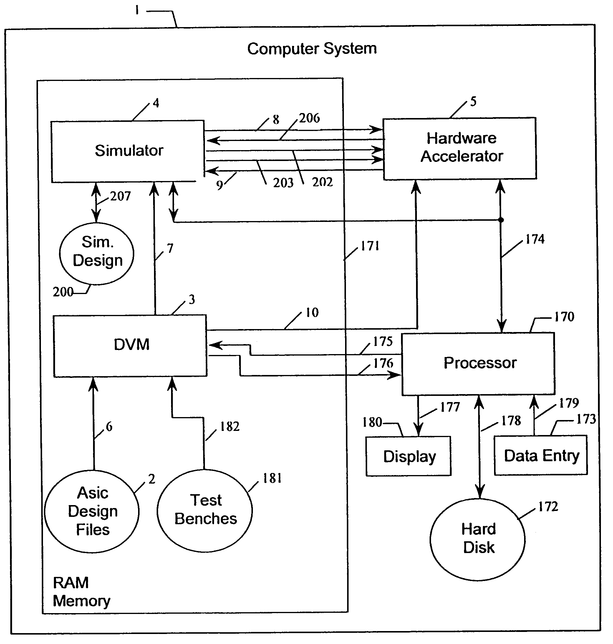
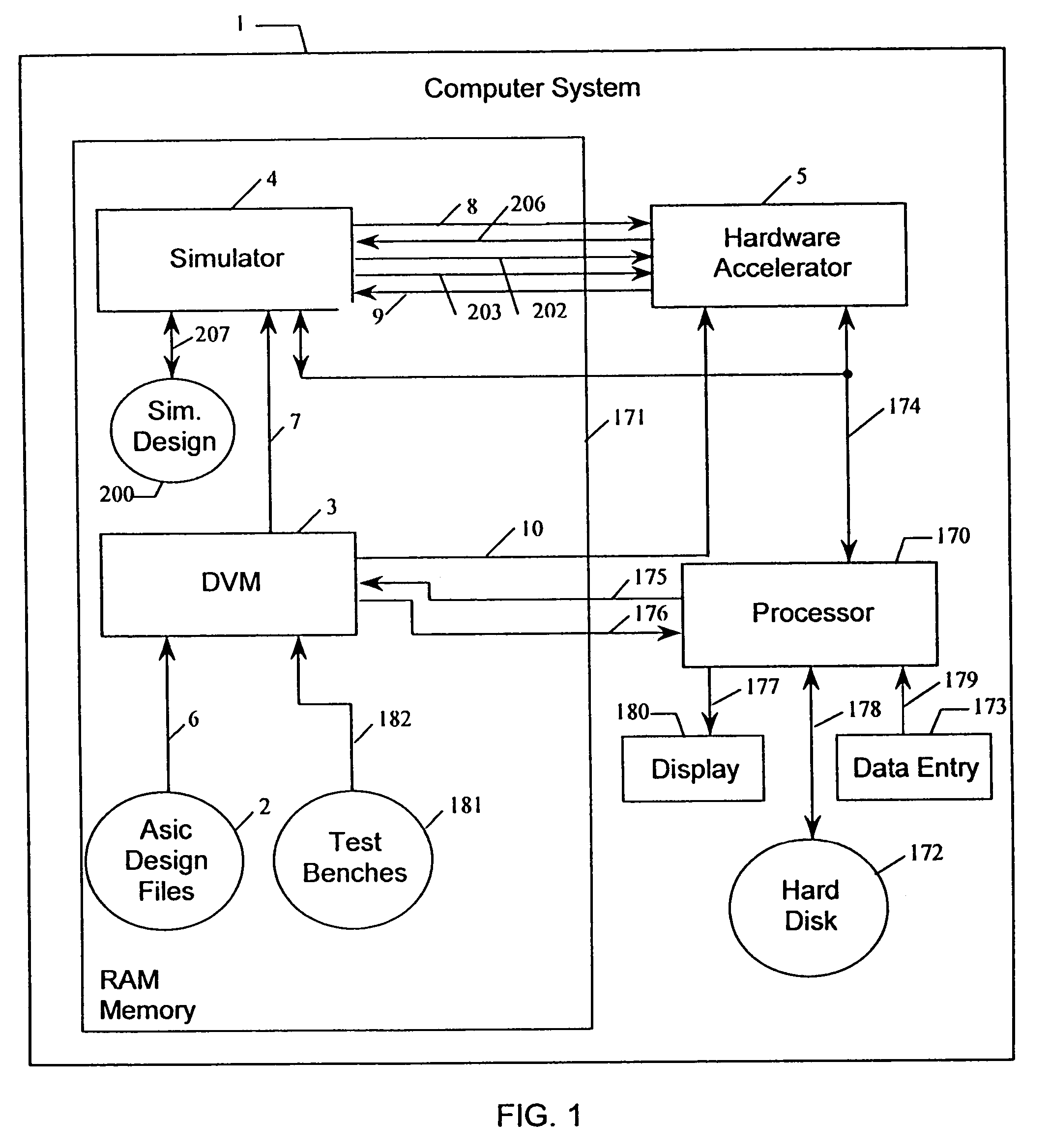
[0041]A block diagram illustrating a computer system 1 for design verification and automatic ASIC prototyping by means of reprogrammable devices is illustrated in FIG. 1. Computer system 1 can be a workstation such as a SunBlade 1000 manufactured by Sun Microsystems or a personal computer (PC) available from a number of manufacturers such as Dell, Hewlett-Packard, etc. Computer system 1 is comprised of processor 170, random access memory (RAM) 171, hard disk storage 172, data entry device 173 and display or monitor 180. While a variety of input devices or data entry devices can be used for simplicity, we will refer to data entry device 173 most frequently as a keyboard.

[0042]In addition, computer system 1 includes software simulator 4 residing in computer memory 171, a reprogrammable hardware accelerator 5 comprised of one or more reprogrammable devices that can be programmed with design sections, and Design Verification Manager (DVM) software 3 for converting ASIC designs to a form...


PUM


Abstract

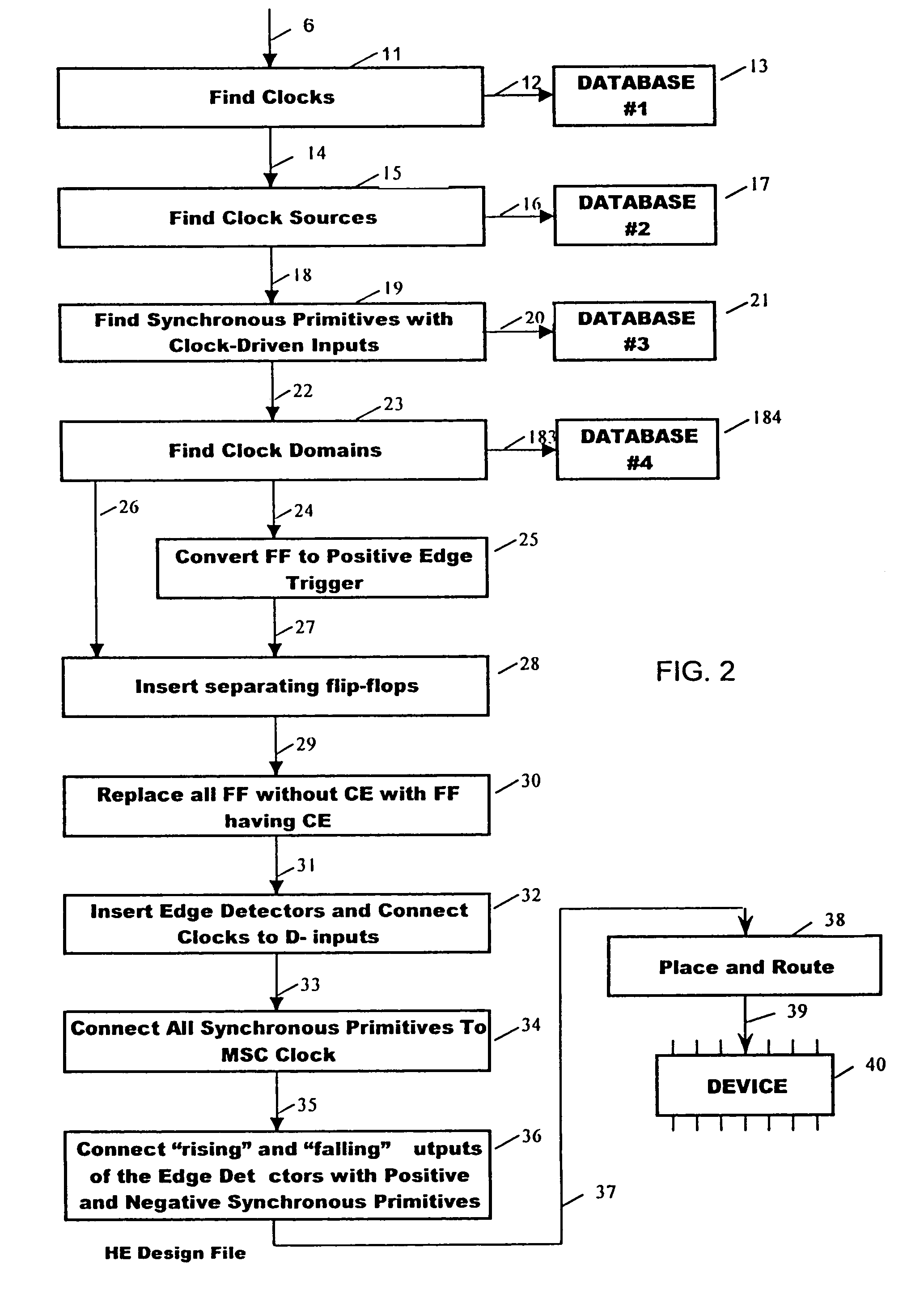
A method and system for accelerating software simulator operation with the aid of reprogrammable hardware such as Field Programmable Gate Array devices (FPGA). The method and system aid in emulation and prototyping of Application Specific Integrated Circuits (ASIC) digital circuit designs by means of reprogrammable devices. The system includes a design verification manager and software program that includes subroutines of finding clock sources, finding synchronous primitives that are receiving clock signals from the clock sources, and a subroutine for inserting edge detector circuits between such clock sources and synchronous primitives. This new method allows eliminating of clock timing issues by applying basic design clocks to the clock enable instead of clock trigger inputs and generating and applying to clock trigger inputs a new clock that is automatically delayed in respect to all other clocks in the design. This system solves the major obstacle for automatic retargeting of ASIC designs into reprogrammable devices that have different timings of the clocking chains in ASICs and FPGAs that result in triggering of associated flip-flops and latches at different times.

Description

BACKGROUND OF THE INVENTION[0001]1. Field of the Invention[0002]The present invention relates to verification of electronic circuit designs and more particularly to accelerating verification of current circuit design by the acceleration of software simulators and emulation of electronic designs by means of reprogrammable devices such as a Field Programmable Gate Array (FPGA). More particularly the invention can relate to the accelerated verification by automatic retargeting of Application Specific Integrated Circuits (ASIC) designs and High Definition Logic (HDL) designs in general, into reprogrammable devices of the specified kind.[0003]2. Background Information[0004]Today's ASIC designs have tens of millions of gates. To verify these designs, software simulators such as the NC-Sim from Cadence Design, VCS Simulator from Synopsys and Riviera and an Active-HDL from Aldec, Inc. of Las Vegas, Nev. may be used. However, since the number of gates in ASIC designs is growing faster than t...

Claims


Application Information

Patent Timeline
Patent Type & Authority Patents(United States)
IPC IPC(8): G06F17/50G06F7/62G06F9/45G06F9/455
CPCG06F17/5027G06F30/331
Inventor HYDUKE, STANLEY M.GRABOWSKI, SLAWOMIR
Owner HYDUKE STANLEY M
Learn More