
Substrate processing apparatus and method of processing substrate while controlling for contamination in substrate transfer module

Inactive Publication Date: 2006-02-07
SAMSUNG ELECTRONICS CO LTD
View PDF14 Cites 48 Cited by
  • Summary
  • Abstract
  • Description
  • Claims
  • Application Information

AI Technical Summary

Benefits of technology

[0024]More specifically, an object of the present invention is to provide a substrate processing apparatus and method by which the level of contaminants within a substrate transferring module can be controlled.
[0025]Another object of the present invention is to prevent substrates from being contaminated while they are standing by in a container, such as a FOUP, as other substrates are being processed and subsequently loaded into the FOUP.
[0026]Yet another object of the present invention is to prevent substrates from being contaminated while they are being transferred in a closed container, such as a FOUP, after being dry etched or the like in a substrate processing apparatus.
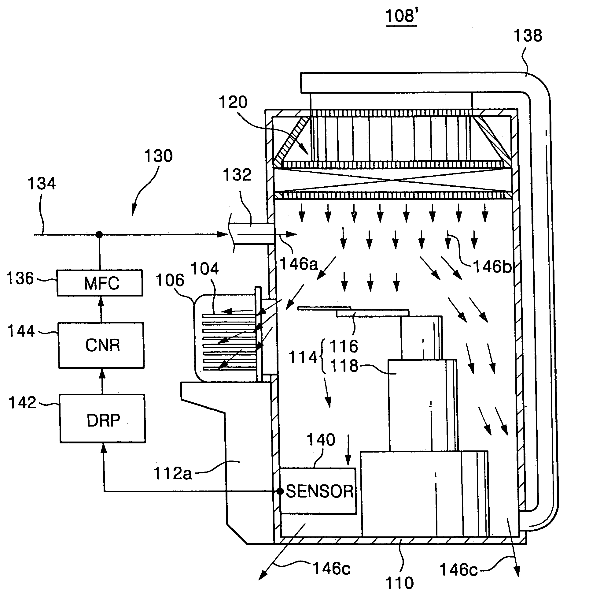
[0030]According to the present invention, a purging gas, such as nitrogen gas, is supplied to the substrate transfer chamber of the substrate transferring module for transferring substrates from a container to one or more substrate processing chambers. The purging gas is also re-circulated through the substrate transfer chamber to remove moisture and various airborne molecular contaminating materials (AMC) including ozone from the substrate transfer chamber. Therefore, the condensate can be prevented from forming on the processed wafers while they are standing by in a container as more processed wafers are being processed and loaded into the container.
[0031]Also, a container supported by the load port of the substrate transferring module can be filled with purging gas from the substrate transferring chamber during the loading of substrates into or the unloading of the substrates from the container. In either case, contaminating materials are thus prevented from flowing into the container. In particular, moisture and contaminating materials in the ambient can be prevented from flowing into the container during transferring of the container to another apparatus for performing the next process on the wafers.

Problems solved by technology

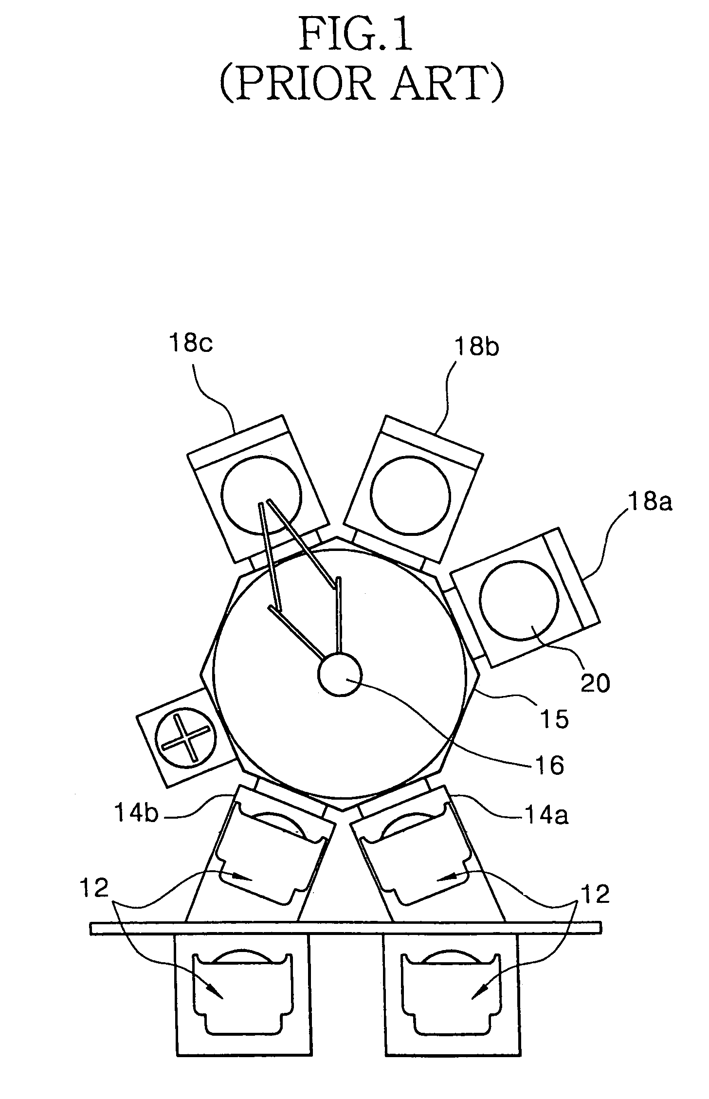
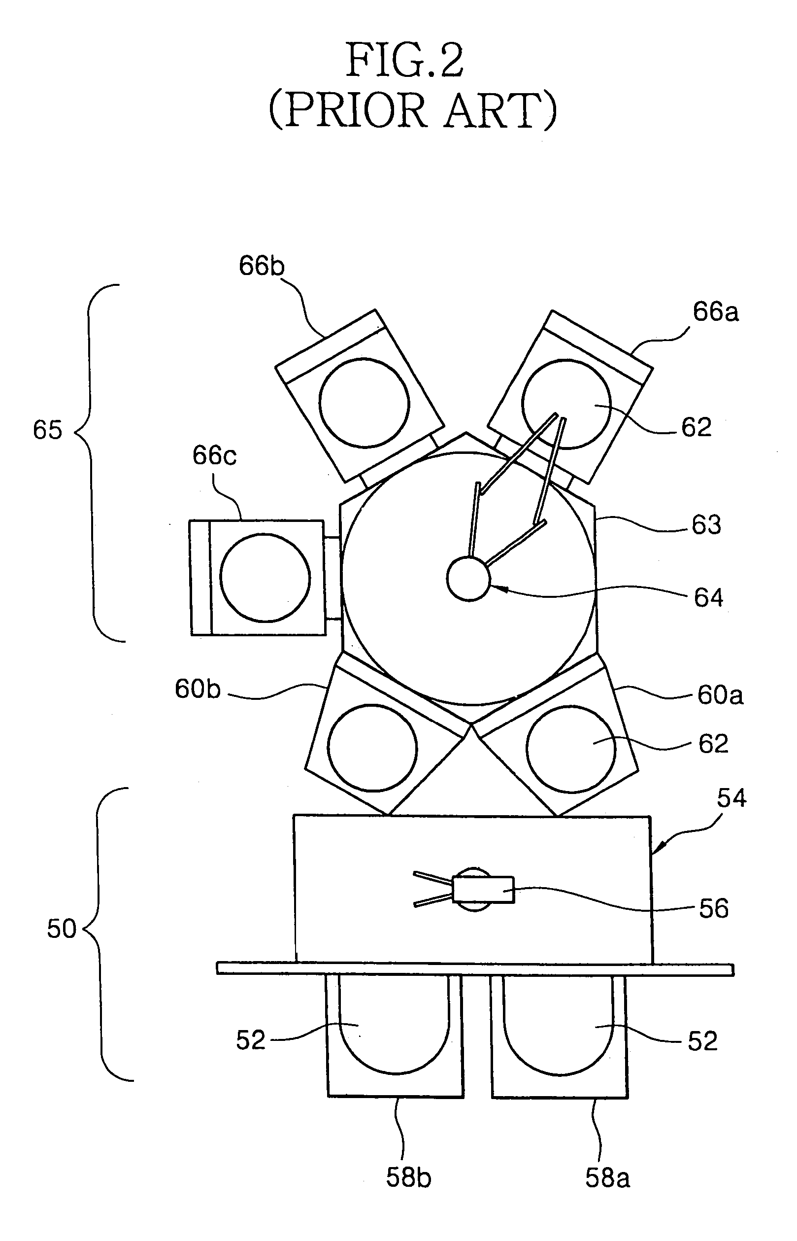
However, a considerable amount of time is required for creating the high vacuum state in the processing chamber, i.e., for reducing the pressure from atmospheric pressure to a high vacuum pressure.
Therefore, when the FOUP is introduced into the low-vacuum loadlock chamber, a large amount of time is required to reduce the pressure in the loadlock chamber from atmospheric pressure to a low vacuum pressure.
Likewise, a large amount of time is required to subsequently increase the pressure in the loadlock chamber from the low vacuum pressure to atmospheric pressure.
Therefore, the efficiency of the dry etching process using this type of apparatus is relatively low.
Thus, the processing of the 300 mm wafers requires a great deal of time.
Therefore, such long delay times allow for the contamination of the wafer to intensify.
Moreover, the contamination is particularly deleterious when the pattern on the wafer is minute, i.e., has a small critical dimension.
For instance, particles of ozone can facilitate the growth of a natural oxide layer and thereby increasing the resistance of the pattern, and moisture can cause a gate oxide layer to deteriorate.
However, the loadlock chamber of this apparatus must have a large volume to accommodate the relatively large FOUP.
Hence, a great deal of time is required for forming a vacuum in the loadlock chamber of this apparatus.
Accordingly, the efficiency of the apparatus is rather low.

Method used


Image

  • Substrate processing apparatus and method of processing substrate while controlling for contamination in substrate transfer module
  • Substrate processing apparatus and method of processing substrate while controlling for contamination in substrate transfer module
  • Substrate processing apparatus and method of processing substrate while controlling for contamination in substrate transfer module

Examples


Embodiment Construction

[0041]Hereinafter, the preferred embodiments of the present invention will be described in detail with reference to the attached drawings. The same reference numeral designate like parts throughout the drawings.

[0042]Referring first to FIG. 5, a dry etching apparatus for etching 300 mm wafers includes a substrate transferring module 108, low-vacuum loadlock chambers 122a and 122b and a substrate processing section 102.

[0043]The substrate processing section 102 includes a plurality of high-vacuum processing chambers 128a, 128b and 128c, a transferring chamber 124, and a transferring robot 126 disposed in the transferring chamber 124. Wafers 104 having a diameter of 300 mm, for example, are transferred between the loadlock chambers 122a and 122b and the processing chambers 128a, 128b and 128c by the transferring robot 126. Predetermined processes, such as dry etching processes, are carried out on the wafers 104 in the processing chambers 128a, 128b and 128c.

[0044]Referring now to bot...


PUM


Abstract

A substrate processing apparatus for processing substrates prevents the substrates from contaminating as they are transferred. The apparatus includes a container, like a FOUP, for containing substrates, at least one processing chamber where the substrates are processed, a substrate transferring module including a substrate transfer chamber and at least one load port for supporting a container, and a contamination controlling system for the substrate transfer chamber. The contamination controlling system includes a purge gas supply inlet connected to the substrate transfer chamber, and a gas circulating tube for recycling the purging gas to circulate through the chamber. The substrate transfer chamber is purged using the purging gas to remove moisture and contaminating materials from the substrate transfer chamber. The formation of particles on the substrate otherwise caused by a reaction between the moisture and contaminating materials while the substrate is standing by in the container can be prevented.

Description

BACKGROUND OF THE INVENTION[0001]1. Field of the Invention[0002]The present invention relates to a substrate processing apparatus and to a method of transferring the substrate to a processing chamber of the apparatus. More particularly, the present invention relates to a substrate transfer module for transferring a substrate from a container to a substrate processing chamber.[0003]2. Description of the Related Art[0004]The manufacturing of semiconductor devices generally includes a photolithographic process in which a photoresist pattern is formed on a wafer, and a dry etching process in which the wafer is subsequently etched using the photoresist pattern as an etching mask. The dry etching process is performed in a processing, chamber under a high vacuum state. However, a considerable amount of time is required for creating the high vacuum state in the processing chamber, i.e., for reducing the pressure from atmospheric pressure to a high vacuum pressure. Therefore, a low-vacuum lo...

Claims


Application Information

Patent Timeline
IPC IPC(8): G06F7/00B65G49/07H01L21/68H01L21/00H01L21/673H01L21/677
CPCH01L21/00Y10S414/139H01L21/67017H01L21/68
Inventor AHN, YO-HANKIM, KI-DOOLEE, SOO-WOONGHWANG, JUNG-SUNGKIM, HYEOG-KI
Owner SAMSUNG ELECTRONICS CO LTD
Learn More