
Display device and method of fabricating the display device

a display device and display device technology, applied in the field of display devices, can solve the problems of reducing yield or image quality, unable to apply the display potential to the cathode, and unable to achieve the effect of preventing discontinuity in el film or electrode, and forming the film forming surface smoothly

Inactive Publication Date: 2006-02-07
SEMICON ENERGY LAB CO LTD
View PDF30 Cites 143 Cited by
  • Summary
  • Abstract
  • Description
  • Claims
  • Application Information

AI Technical Summary

Benefits of technology

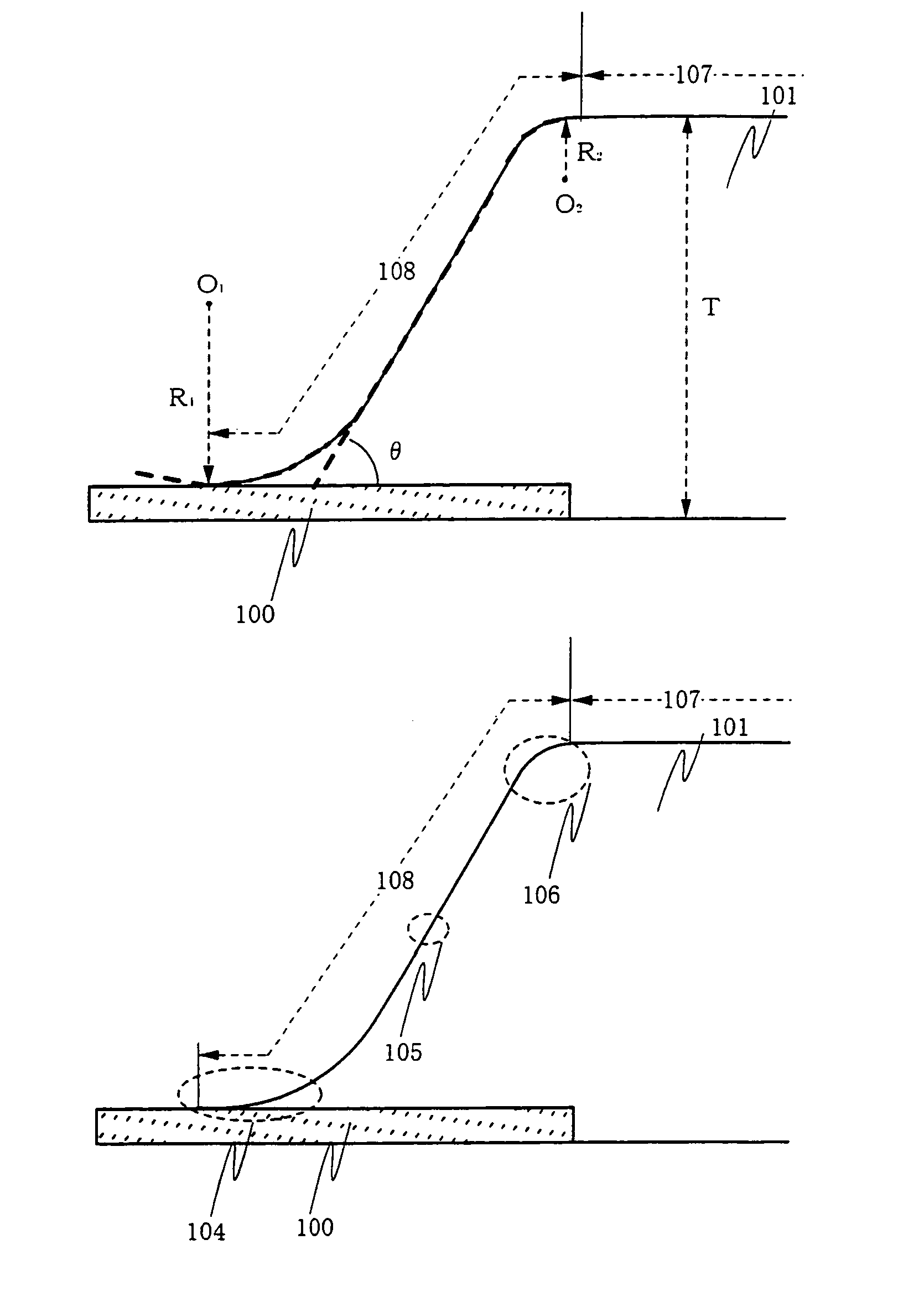
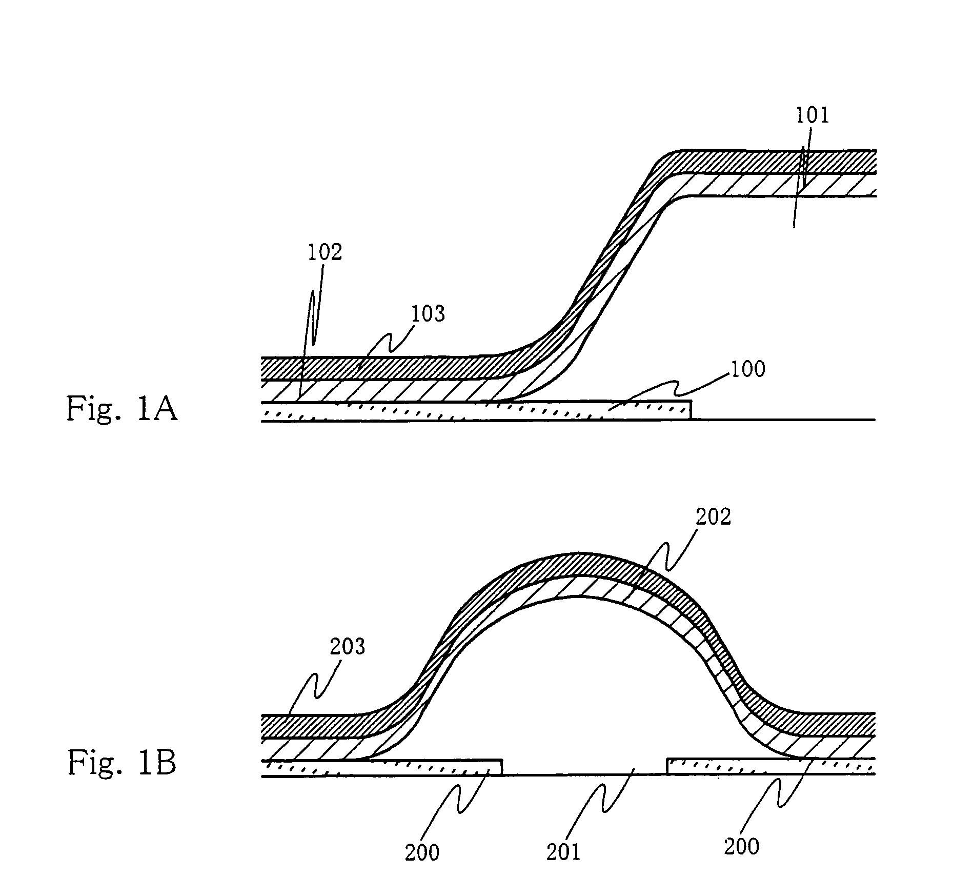
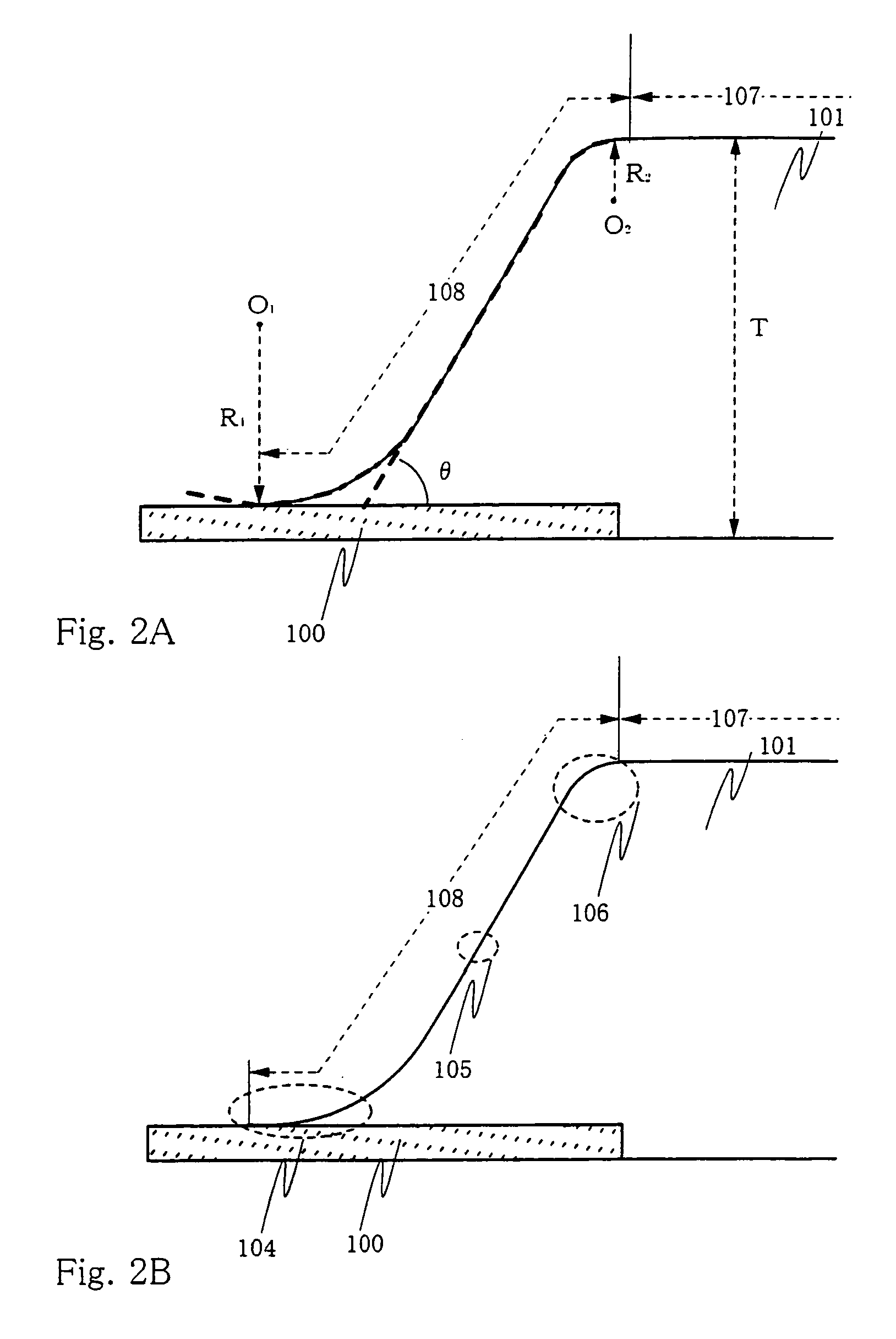
[0017]An object of the present invention is to provide a display device in which occurrence of discontinuity in an EL film or an electrode is prevented by smoothly forming the film forming surface, and a method of fabricating the display device.
[0018]The inventors of the present invention conceived that a method of smoothly changing, through optimization of the shape of the bump, the gradient of the film forming surface of the bump on which the EL film and the cathode are formed could be effective in improving the facility with which the EL film and the cathode are formed so as to be uniform in thickness and in reducing the occurrence of discontinuity in each of the EL film and the cathode as well as in reducing the amount by which the EL film is locally reduced in thickness. The inventors then optimized the shape of the bump to enable the EL film and the cathode to be formed so as to be uniform in thickness and to achieve improved display performance.

Problems solved by technology

If a discontinuity is caused in the EL film, the anode and the cathode are short-circuited, light emission from the corresponding EL film portion is thereby made impossible, and a black-dot defect results.
The structure shown in the cross-sectional view of FIG. 18, however, entails several problems in an actual fabrication process.
In a case where the cathode on the insulating film is electrically connected to a wiring below the insulating film via a contact hole formed through the insulating film, discontinuity in the cathode at the side surface of the insulating film may cause failure to apply the necessary potential for display to the cathode.
That is, a point defect results.
In manufacture of display devices using EL elements in which the number of pixels is increased to improve the resolution, the occurrence of point defects due to short-circuiting between the anodes and cathode or due to discontinuity in the cathode is a factor which causes a reduction in yield or in image quality, and there is an urgent need to cope with this problem.
Also, convergence of the electric field due to the state of the EL film locally reduced in thickness makes the luminance of the defective pixel portion different from that of nondefective pixel portion, resulting in a reduction in viewability.

Method used


Image

  • Display device and method of fabricating the display device
  • Display device and method of fabricating the display device
  • Display device and method of fabricating the display device

Examples


embodiment 1

(Embodiment 1)

[0120]The present invention can be applied to all display devices using EL elements. FIG. 8 shows an example of a display device using EL elements, which is an active matrix display device fabricated by using TFTs. TFTs may be separated into amorphous silicon TFTs and polysilicon TFTs according to the semiconductor film material for forming the channel forming region. However, the present invention can be applied to either of display devices using amorphous silicon TFTs and display devices using polysilicon TFTs.

[0121]FIG. 8 shows a state where an n-channel TFT 452 and a p-channel TFT 453 are formed in a drive circuit portion 450, and a switching TFT 454 and a current control TFT 455 are formed in a pixel portion 451. These TFTs are formed by using semiconductor layer lands 403 to 406, gate insulating film 407, gate electrodes 408 to 411, etc.

[0122]A substrate formed of glass such as barium borosilicate glass or alumino borosilicate glass typified by #7059 glass or #17...

embodiment 2

(Embodiment 2)

[0147]FIG. 13 shows an example of a display device using inverse staggered TFTs. A substrate 501 and EL elements 556 used in this embodiment are the same as those of Embodiment 1, and the description for them will not be repeated.

[0148]In the inverse staggered TFTs, gate electrodes 508 to 511, gate insulating film 507, and semiconductor films 503 to 506 are formed in this order on the substrate 501. As shown in FIG. 13, n-channel TFT 552 and p-channel TFT 553 are formed in a drive circuit portion 550, and switching TFT 554, current control TFT 555 and EL element 556 are formed in a pixel portion 551. An interlayer insulating film is formed of an inorganic insulating film 518 formed by silicon nitride, silicon oxynitride or the like and an organic insulating film 519 formed by acrylic, polyimide or the like.

[0149]The drive circuit portion 550 has different circuit configurations with respect to a gate signal drive circuit and a data signal drive circuit. The difference ...

embodiment 3

(Embodiment 3)

[0154]An example of an electronic device using the display device described above as Embodiment 1 will be described with reference to FIG. 14. In the display device shown in FIG. 14, TFTs formed on a substrate constitute a pixel portion 921 having pixel portion 920, a data signal drive circuit 915 used to drive the pixel portion, and a gate signal drive circuit 914. The data signal drive circuit 915 is shown as an example of a digital drive and is constituted by a shift register 916, latch circuits 917 and 918, and a buffer circuit 919. The gate signal drive circuit 914 has a shift register, a buffer, etc., (each not shown).

[0155]The pixel portion 921 has 640 (in horizontal direction)×480 (in vertical direction) pixel portion if it is of the Video Graphics Array (VGA) type. As described above with reference to FIG. 8 or FIGS. 9A and 9B, a switching TFT and a current control TFT are provided in each pixel portion. Each EL element operates in such a manner that when the ...


PUM


Abstract

In an EL element having an anode, an insulating film (bump) formed on the anode, and an EL film and a cathode formed on the insulating film, each of a bottom end portion and a top end portion of the insulating film is formed so as to have a curved surface. The taper angle of a central portion of the insulating film is set within the range from 35° to 70°, thereby preventing the gradient of the film forming surface on which the EL film and the cathode are to be formed from being abruptly changed. On the thus-formed film forming surface, the EL film and the cathode can be formed so as to be uniform in thickness, so that occurrence of discontinuity in each of EL film and the cathode is prevented.

Description

[0001]This application is a continuation of U.S. application Ser. No. 10 / 827,709, filed on Apr. 20, 2004 which is a divisional of U.S. application Ser. No. 09 / 953,765 filed on Sep. 17, 2001 (now U.S. Pat. No. 6,739,931 issued May 25, 2004).BACKGROUND OF THE INVENTION[0002]1. Field of the Invention[0003]The present invention relates to a display device including an element having a thin film of a chemical compound capable of electroluminescence (EL) (which film hereinafter referred to as “EL film”) (which element hereinafter referred to as “EL element”), and to a method of fabricating the display device.[0004]EL comprises phosphorescence caused at the time of transition from a triplet excited state to a ground state and fluorescence caused at the time of transition from a singlet excited state to a ground state.[0005]An inorganic material or an organic material may be used to form an EL film. “Organic EL film” refers to a film of an organic material formed as an EL film. “Organic EL ...

Claims


Application Information

Patent Timeline
Patent Type & Authority Patents(United States)
IPC IPC(8): H01J1/62H01L27/32
CPCH01L27/3246H01L27/124H01L27/1248H01L27/323H01L27/1214Y10S428/917H10K59/122H10K59/40
Inventor YAMAZAKI, SHUNPEISUZAWA, HIDEOMIUEHARA, ICHIRO
Owner SEMICON ENERGY LAB CO LTD
Learn More