Secure encryption processor with tamper protection

Inactive Publication Date: 2006-01-31
FUJITSU LTD
View PDF23 Cites 16 Cited by
  • Summary
  • Abstract
  • Description
  • Claims
  • Application Information

AI Technical Summary

Benefits of technology

[0017]By checking the coincidence, an unauthorized access can be prevented. Also, because unnecessary components are not operating in the standby mode, waste of power consumption can be reduced.
[0021]By storing more than one main program in the ROM, the encryption control apparatus can be used extensively, and by allowing only one of the main programs to run selectively at the start-up from the standby status, the interference of the main programs can be avoided, thereby ensuring data security and job reliability.
[0025]According to the above arrangement, privacy and safety of the private key can be maintained, thereby making illegal deciphering of the data more difficult.
[0035]By checking the coincidence, an unauthorized access can be prevented. Also, by enabling the I / O section only when it has to be operated, not only can the security be ensured further, but also the power consumption can be saved. Further, by controlling the security level as described above, an unnecessary access can be prevented, thereby further ensuring the security.
[0039]According to the above arrangement, illegal delivery of the key to an intruder can be prevented.

Problems solved by technology

However, when an encryption / decryption computation is carried out by a general information processing device, it is difficult to conceal an encryption / decryption algorithm or a key used in encrypting / decrypting data.
Therefore, such an algorithm or a key may be leaked illegally, resulting in unauthorized tampering with the data.
Also, because the conventional I / O control unit for controlling the peripherals, such as the IC card reader / writer, is composed of a plurality of semiconductor devices, progress information of the I / O control job is outputted to an address bus or a data bus interconnecting the semiconductor devices, thereby exposing such information to the risk of stealing.
As has been discussed, the conventional technique poses a problem in data security, and there has been an increasing need to ensure the security.

Method used


Image

  • Secure encryption processor with tamper protection
  • Secure encryption processor with tamper protection
  • Secure encryption processor with tamper protection

Examples


first embodiment

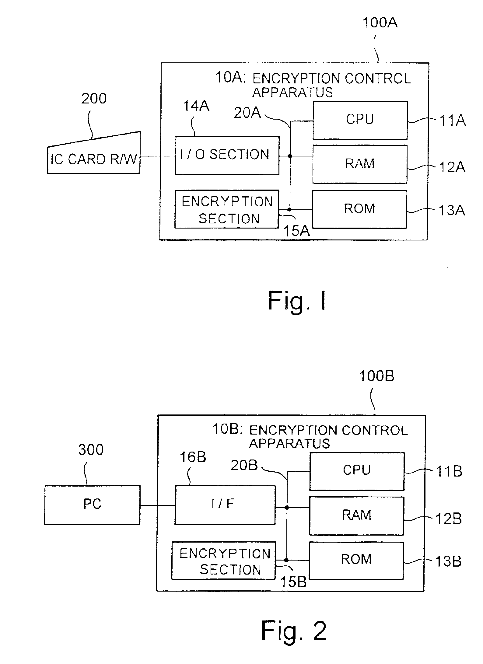
[0053]FIG. 1 is a block diagram showing an encryption control apparatus of the present invention.

[0054]An encryption control apparatus 10A is formed in a single semiconductor device 100, and comprises a CPU 11A for running the program, a RAM 12A used as a work area while the CPU 11A is running a program, a ROM 13A for storing the program run by the CPU 11A, an I / O section 14A for sending / receiving data to / from an external device (herein, IC card reader / writer (IC card R / W) 200), and an encryption section 15A for decrypting encrypted data and encrypting plain text data. The components forming the encryption control apparatus 10A are interconnected to each other through an internal bus 20A.

[0055]The ROM 13A stores an encryption algorithm or a program controlling the I / O section 14A.

[0056]Also, data transmitted between the IC card R / W 200 and I / O section 14A includes control data for controlling the IC card R / W 200 and encrypted data read out from the IC card. The data is encrypted by ...

third embodiment

[0066]FIG. 4 is a view schematically showing a program structure in the ROM in the encryption control apparatus of the present invention.

[0067]The encryption control apparatus of the third embodiment is of the same structure as shown in FIG. 2. Thus, the drawing for the present embodiment is omitted and the explanation is given with reference to FIG. 2.

[0068]A program stored in the ROM 13B includes a start-up routine, a main routine dividing routine, and three main routines A, B, and C. Each of the main routines A, B, and C is allowed to refer to their respective information A, B, and C alone. The main routines A, B, and C allow a single encryption control apparatus to operate in different manners by selectively using encryption / decryption control algorithms different from one another.

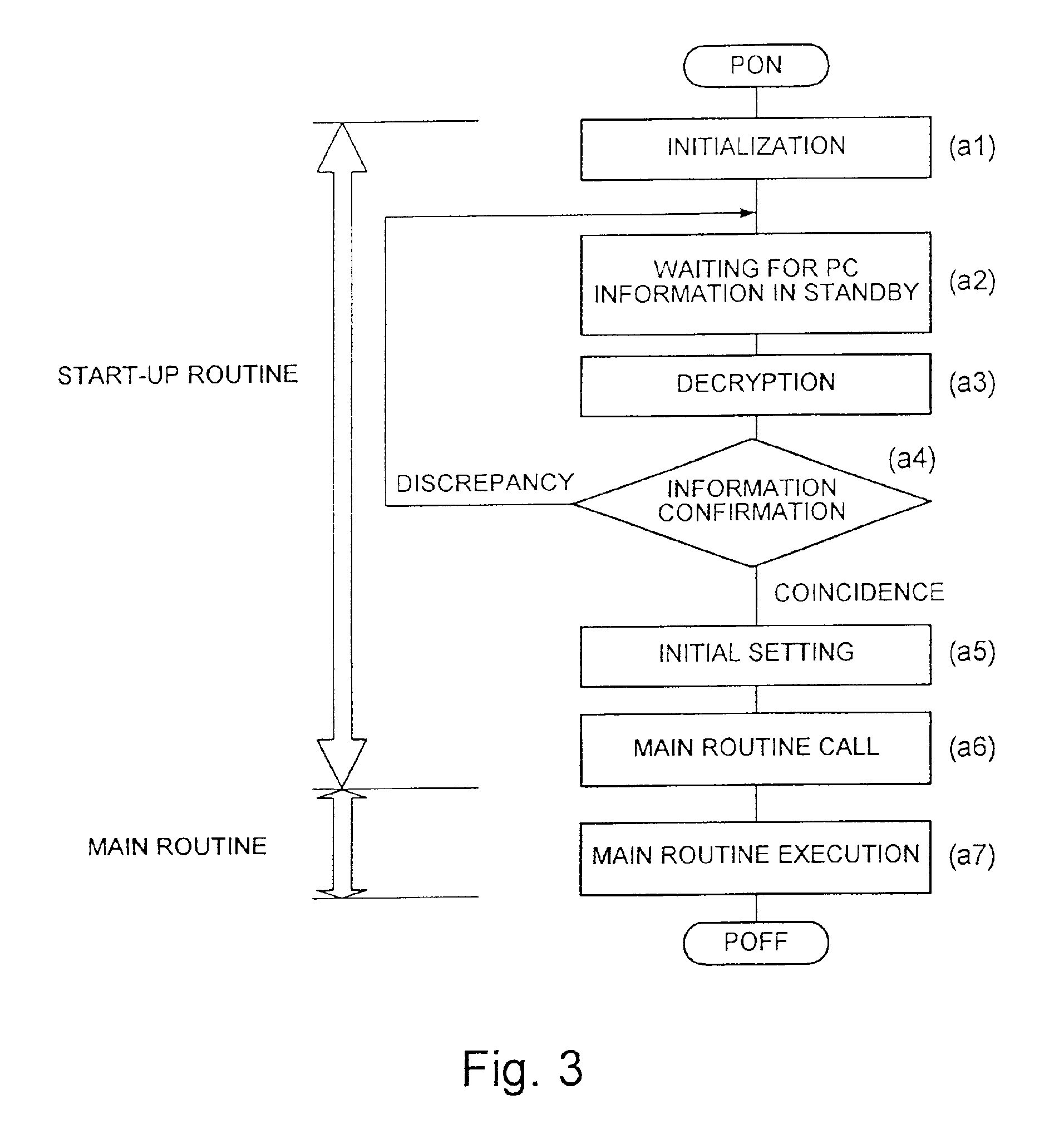
[0069]FIG. 5 is a flowchart showing an operation flow of the third embodiment whose program structure is shown in FIG. 4.

[0070]As is with the operation flow of FIG. 3, the operation flow of FIG. 5 is i...

fourth embodiment

[0074]FIG. 6 is a block diagram showing the encryption control apparatus of the present invention.

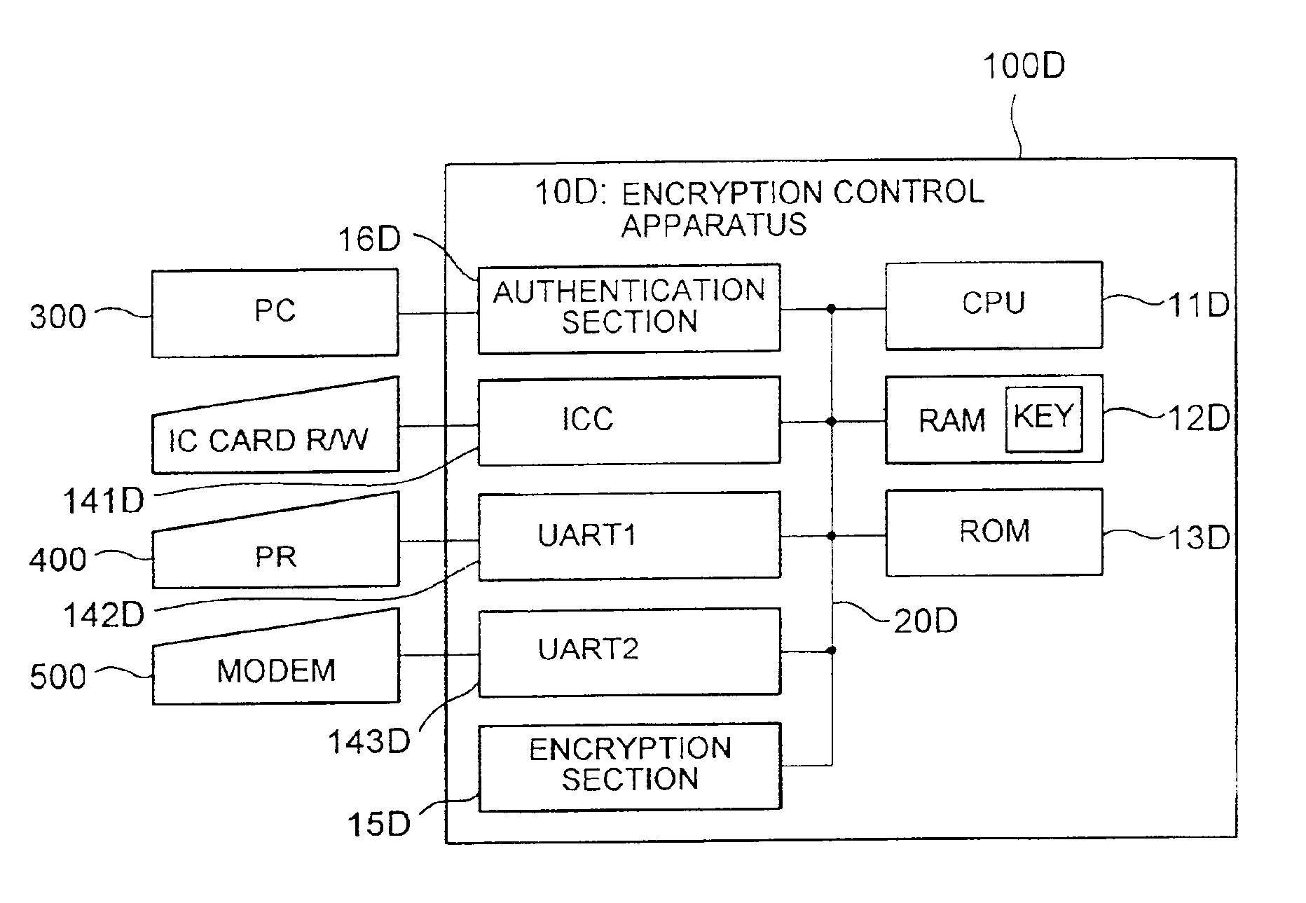
[0075]An encryption control apparatus 10C is formed in a single semiconductor device 100C, and comprises a CPU 11C, a RAM 12C, a ROM 13C, an I / O section 14C, and an encryption section 15C, which are the same as their respective counterparts in the encryption control apparatus 10A of the first embodiment shown in FIG. 1. Hence, the explanation of these components is omitted. FIG. 6 shows schematically but explicitly that the RAM 12C stores a key.

[0076]An authentication unit 16C also forming the encryption control apparatus 10C of FIG. 6 not only serves as an interface connected to the PC 300 to send / receive serial data to / from the PC 300, but also authenticates a data sender to judge whether the data sender is an authorized party or not.

[0077]FIG. 7 is a view showing a data structure of authentication data sent to the encryption control apparatus 10C from the PC 300.

[0078]The authenticat...


PUM


Abstract

An encryption processor for encrypting and decrypting data that ensures data security by preventing illegal deciphering or leakage of the data. The encryption processor includes a CPU for running a program, a ROM for storing the program run by the CPU, a RAM used as a work area while the CPU is running the program, an I / O section for sending / receiving data to / from an external device, and an encryption section for decrypting encrypted data and encrypting plain text data.

Description

BACKGROUND OF THE INVENTION[0001]1. Field of the Invention[0002]The present invention relates to an encryption control apparatus for encrypting and decrypting data.[0003]2. Description of the Related Art[0004]With the recent development of communication techniques, data having the same value as notes, such as electronic money, has been used increasingly, and it becomes quite important to prevent illegal leakage of the data or unauthorized tampering with the data.[0005]As one of the safety measures to protect data, a data encryption and decryption technique has been used, by which data is encrypted when being sent and the receive data is decrypted at the receiver's end. General information processing devices, such as personal computers (hereinafter, abbreviated to PCs occasionally), have been used in encrypting and decrypting data.[0006]Incidentally, attention has been paid to a system that employs an IC card as a typical example of a system capable of dealing with electronic money, ...

Claims


Application Information

Patent Timeline
IPC IPC(8): H04L9/00G06F12/14H04L9/32G06F11/30G06F1/00G06F21/60G06F21/62G06F21/75G06F21/87G06K19/00G07F7/10G09C1/00H04L9/10
CPCG06F21/6209G06F21/72G06F21/85H04L63/0428G06Q20/40975G07F7/082G07F7/1008G07F7/1016G06Q20/341G06F2221/2153
Inventor SEKI, YUJIKAWASAKI, YUSUKEHASHIMOTO, SHIGERUYANAGI, RYOICHI
Owner FUJITSU LTD
Why Eureka
Try Eureka