Laser diode and manufacturing method thereof
a technology of laser diodes and diodes, which is applied in the direction of lasers, semiconductor lasers, solid-state devices, etc., can solve the problems of unsatisfactory reliability, scarce adhesion of films, and high sensitivity to peeling, so as to reduce the resistance to damp, increase the number of surface states, and reduce the effect of sensitivity
- Summary
- Abstract
- Description
- Claims
- Application Information
AI Technical Summary
Benefits of technology
Problems solved by technology
Method used
Image
Examples
example 1
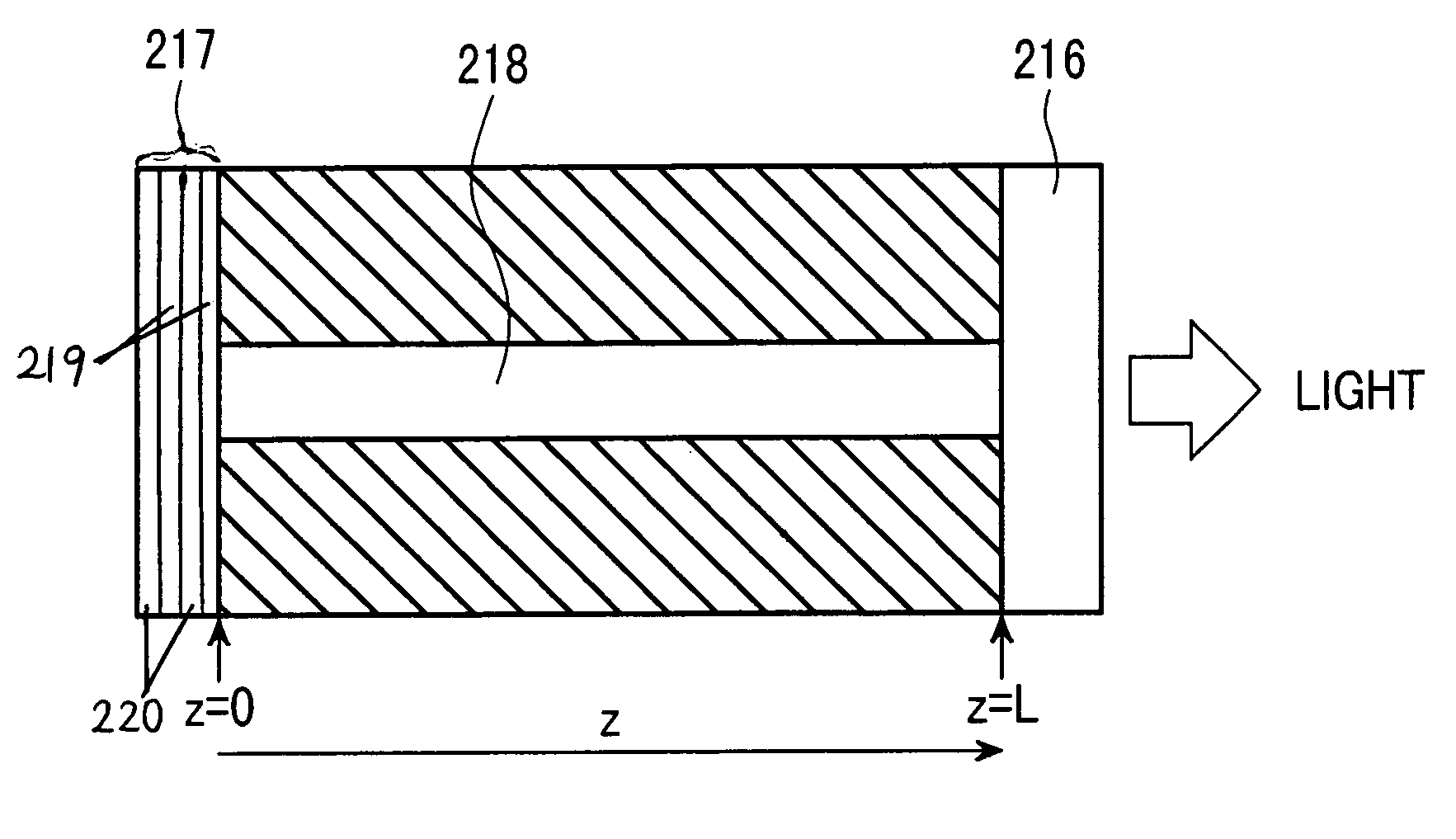
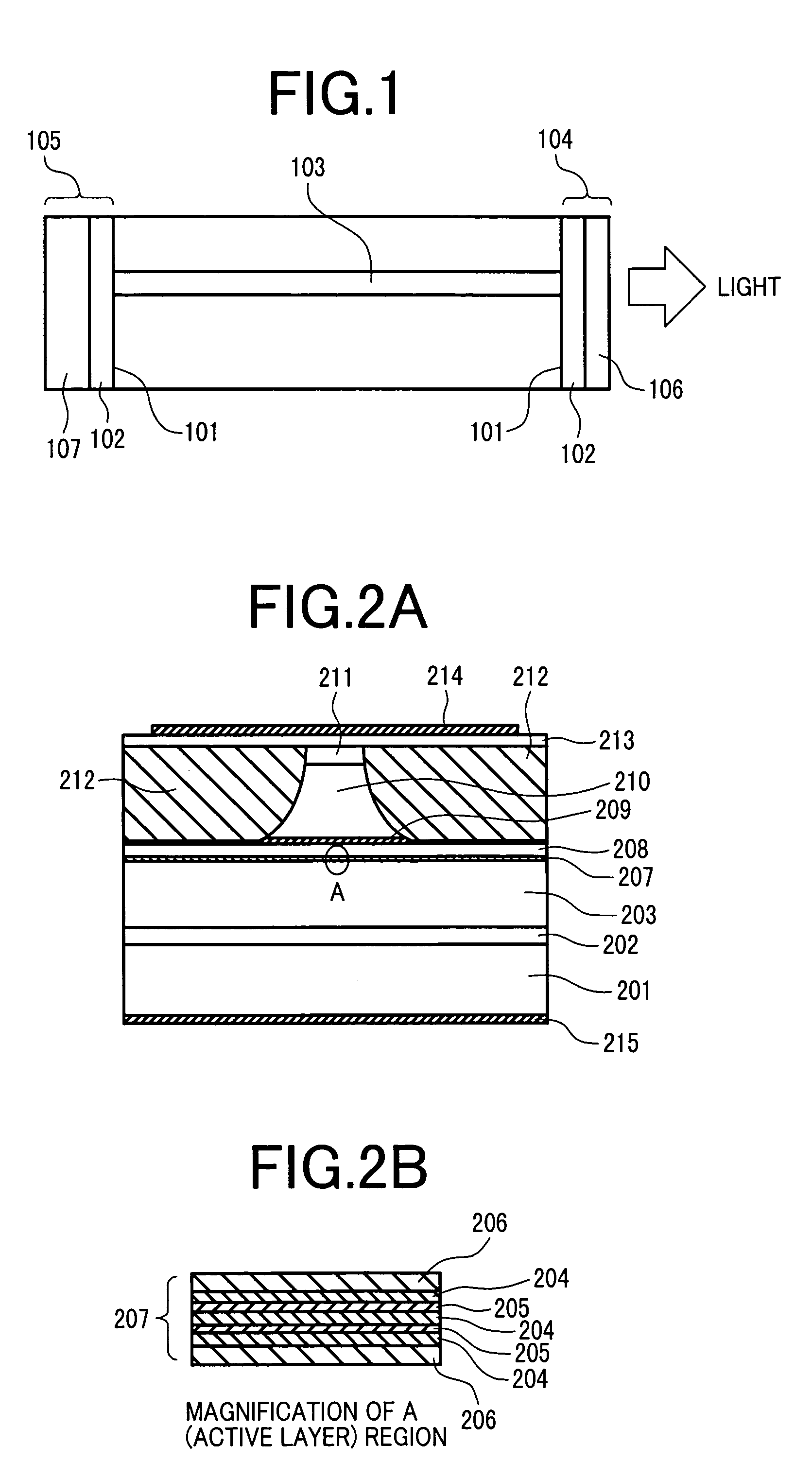
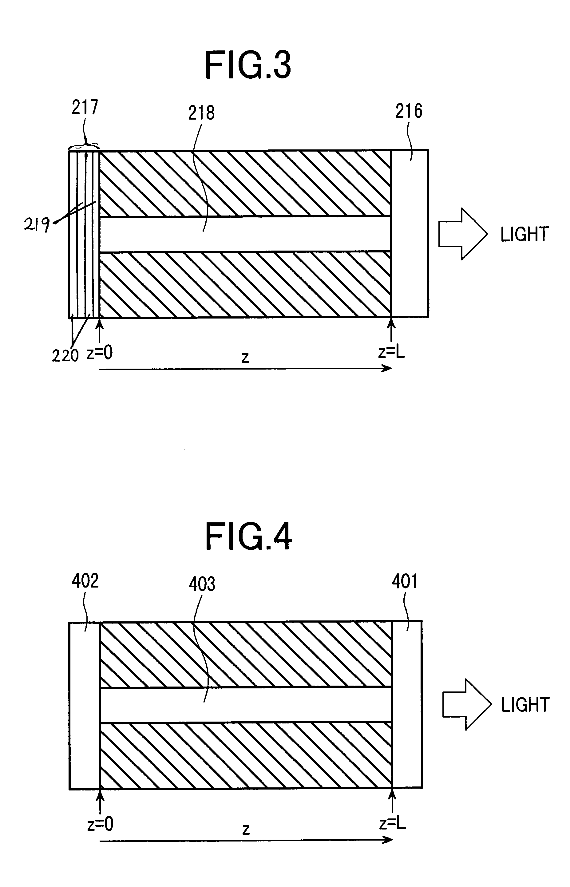
[0038]A first example of the invention is to be explained with reference to FIGS. 2A, 2B and 3. This example is applied to a high power laser diode for 0.65 μm band used for writing in optical disks or magneto-optical disks. FIG. 2A shows a cross-sectional structure, FIG. 2B is an enlarged view of an active layer, and FIG. 3 shows planer structure. Then a device manufacturing method is to be described. On an n-typed GaAs substrate 201, are formed successively, a GaAs buffer layer 202, an n-typed (AlxGa1-x)InP clad layer 203 lattice matched to GaAs (x=0.7), a strained quantum well active layer 207 comprising (AlyGa1-y)InP barrier layers (y=0.45, barrier layer thickness 4 nm) 204 lattice matched to GaAs, InzGa1-zP strained quantum well layers (z ˜0.58, well layer thickness 87 nm) 205, and (AlsGa1-s)Inp SCH (Separate Confinement Heterostructure) layers (s=0.55, barrier wall layer thickness 4 nm) 206, a p-typed (AltGa1-t)InP clad layer (t=0.7) 208 lattice matched to GaAs, a p-typed InGa...
example 2
[0041]A second example of the invention is to be described with reference to FIGS. 4, 5A and 5B. In this example, the invention is applied to a high power laser diode for 0.98 μm band for a rare earth-doped optical fiber amplifier excitation for use in relays or receivers in optical transmitting systems. FIG. 4 shows a planar structure of a laser diode having a Fabry-Pelot type optical resonator, FIG. 5A shows a cross-sectional structure of the same and FIG. 5B shows an enlarged view of an active layer. Then, a device manufacturing method is to be described. On an n-typed GaAs substrate 501, are formed successively, a GaAs buffer layer 502, an n-typed InGaP clad layer 503 latticed matched to GaAs, a strained quantum well active layer 506 comprising In1-xGaxAsyP1-y barrier layers (x=0.82, y=0.63, a barrier layer thickness 35 nm) 504 lattice matched to GaAs, and an InxGa1-zAs strained quantum well layer (z 0.16, well layer thickness 7 mm) 505, a p-typed InGaP clad layer 507 lattice ma...
example 3
[0043]A third example applying the invention is to be explained with reference to FIGS. 6 and 7. In this example, the invention is applied to a laser diode for 1.3 μm band used as a light source in subscriber's optical transmission systems. FIG. 6 is a perspective structure of a laser diode and FIG. 7 shows a cross sectional structure. Then, a device manufacturing method is to be described. After growing an n-typed InP buffer layer 702 on an n-typed InP substrate 601, 701, an n-typed InAlAs clad layer 703 lattice matched to InP, an n-typed InGaAlAs lower SCH layer 704, a strained quantum well active layer 705 comprising an InGaAlAs strained barrier layer (band gap: 1.32 eV, barrier layer thickness: 8 nm) and an InGaAlAs strained quantum well layer. (band gap: 0.87 eV, well layer thickness: 6 nm), a p-typed InGaAlAs upper SCH layer 706 lattice matched to the InP substrate, a p-typed InAlAs first clad layer 707, a p-typed InP second clad layer 708, a p-typed InGaAs cap layer 709, and ...
PUM
 Abstract
Description
Claims
Application Information
 - R&D
- Intellectual Property
- Life Sciences
- Materials
- Tech Scout
- Unparalleled Data Quality
- Higher Quality Content
- 60% Fewer Hallucinations
Browse by: Latest US Patents, China's latest patents, Technical Efficacy Thesaurus, Application Domain, Technology Topic, Popular Technical Reports.
© 2025 PatSnap. All rights reserved.Legal|Privacy policy|Modern Slavery Act Transparency Statement|Sitemap|About US| Contact US: help@patsnap.com


