
Semiconductor device

a technology of integrated circuits and semiconductors, applied in the field of semiconductor integrated circuit devices, can solve the problems of lowering the yield rate of an lsi circuit, increasing the cost of lsi using dram of the circuit of such a structure, and extremely delayed operation frequency in low voltage operation mod

Inactive Publication Date: 2006-01-24
RENESAS ELECTRONICS CORP
View PDF14 Cites 4 Cited by
  • Summary
  • Abstract
  • Description
  • Claims
  • Application Information

AI Technical Summary

Benefits of technology

The present invention is related to a semiconductor device with a memory cell and a sense amplifier. The technical effects of the invention include a first precharge circuit for precharging the first bit line pair to a first potential and a second precharge circuit for precharging the second bit line pair to a second potential. The second circuit is a circuit for amplifying one of the first bit line pair and one of the second bit line pair to a first potential and the other pair to a second potential. The first and second precharge circuits ensure that the first and second bit line pairs are precharged to a specific potential before the memory cell is accessed, which improves the speed and accuracy of the semiconductor device.

Problems solved by technology

This event may grow up to a problem that an yield rate of an LSI circuit is lowered.
As a result, cost of LSI using DRAM of the circuit of such structure rises.
Moreover, when the logic LSI including such DRAM is used in a plurality of operation modes where the power source voltage and the operating frequency vary, the operating frequency in the low voltage operation mode is extremely delayed because the DRAM is included.

Method used


Image

  • Semiconductor device
  • Semiconductor device
  • Semiconductor device

Examples


Embodiment Construction

[0052]The preferred embodiments of the present invention will be explained in detail with reference to the accompanying drawings. Circuit elements forming each function block of the preferred embodiments are formed, although not particularly limited, on only one semiconductor substrate made of single crystal silicon or the like with the well known technology to form CMOSs (complementary MOS transistors). The P-type MOS transistor (MOSFET) can be discriminated by giving a sign ◯ to the gate thereof from an N-type MOS transistor (MOSFET).

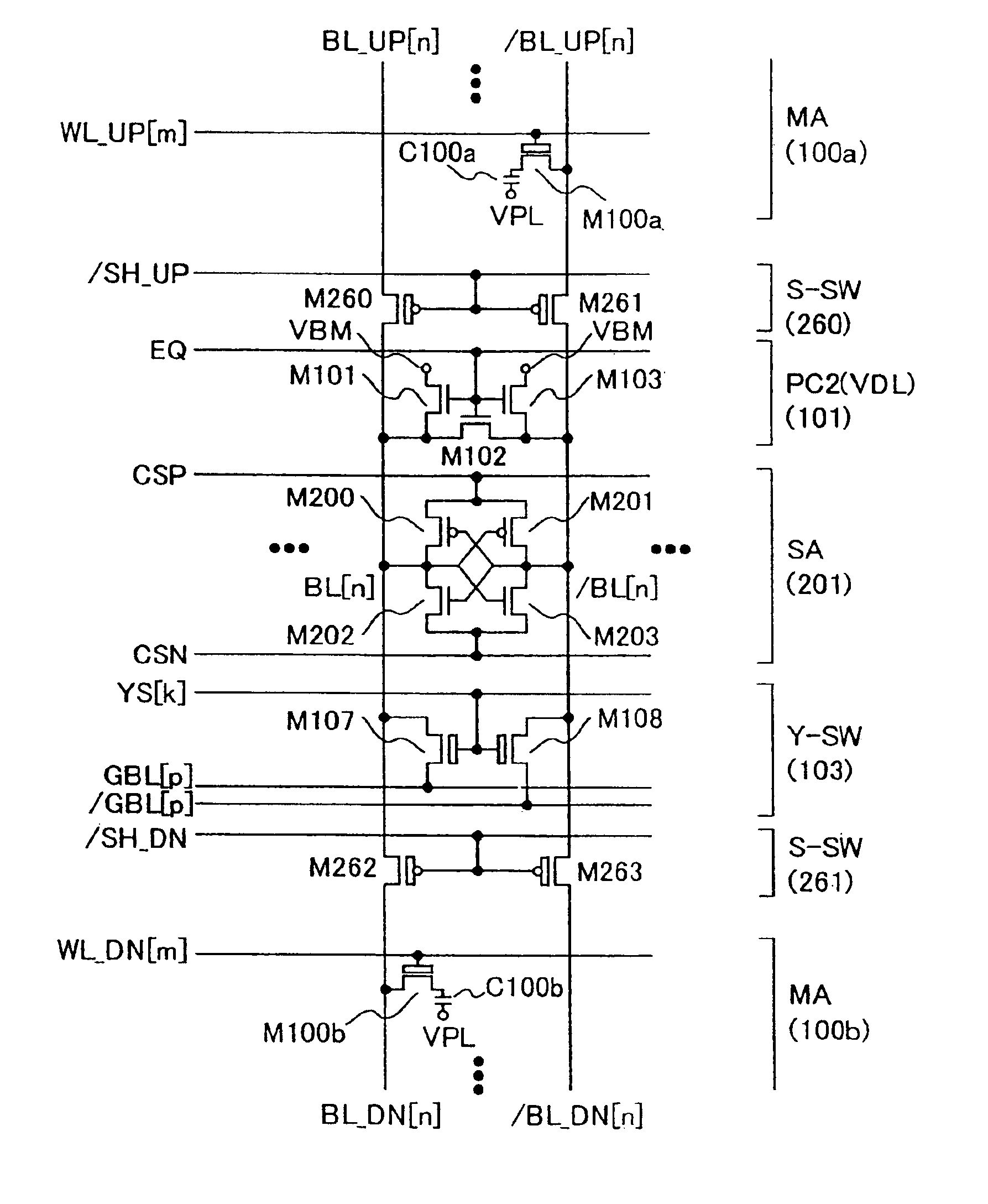
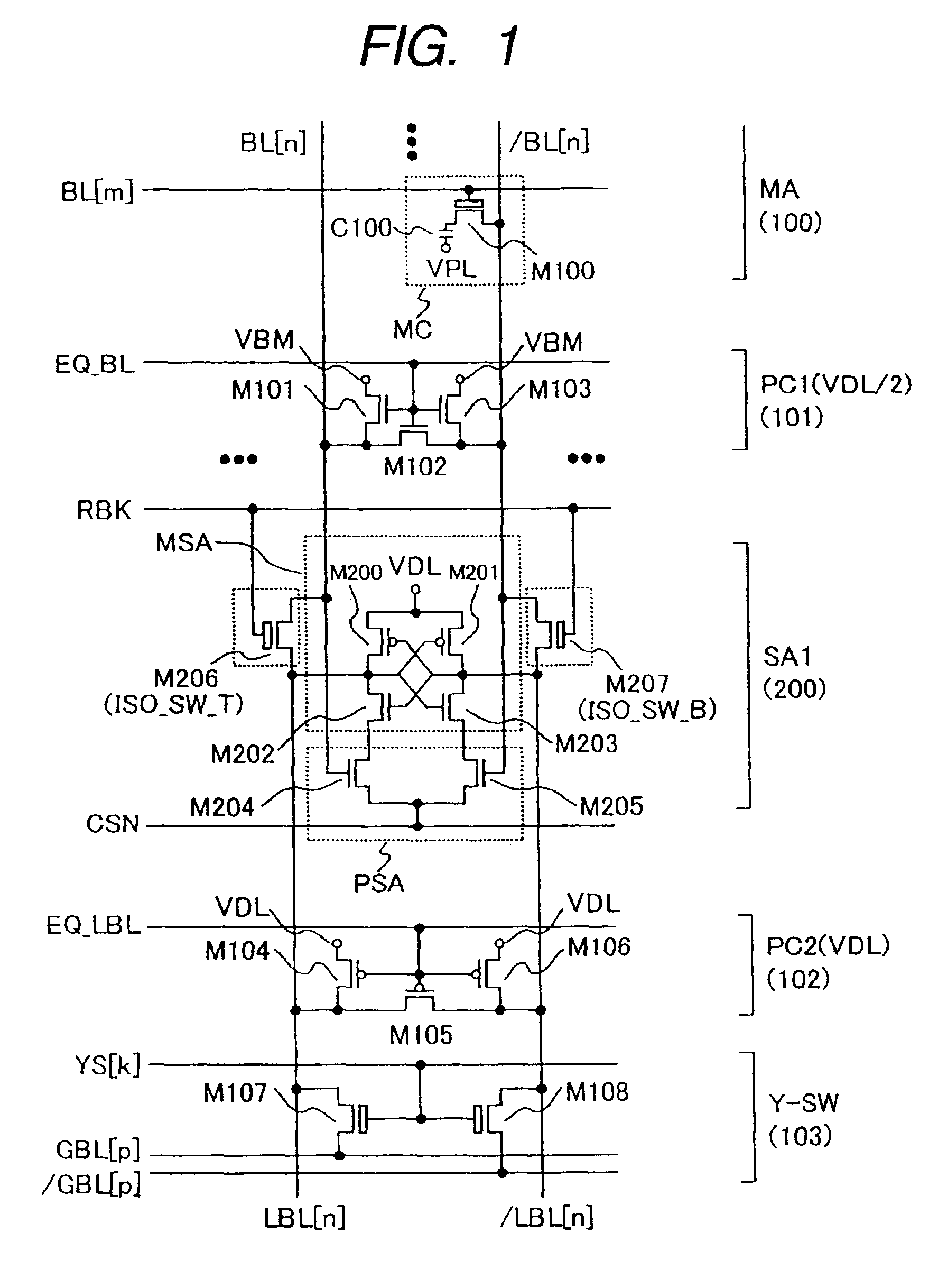
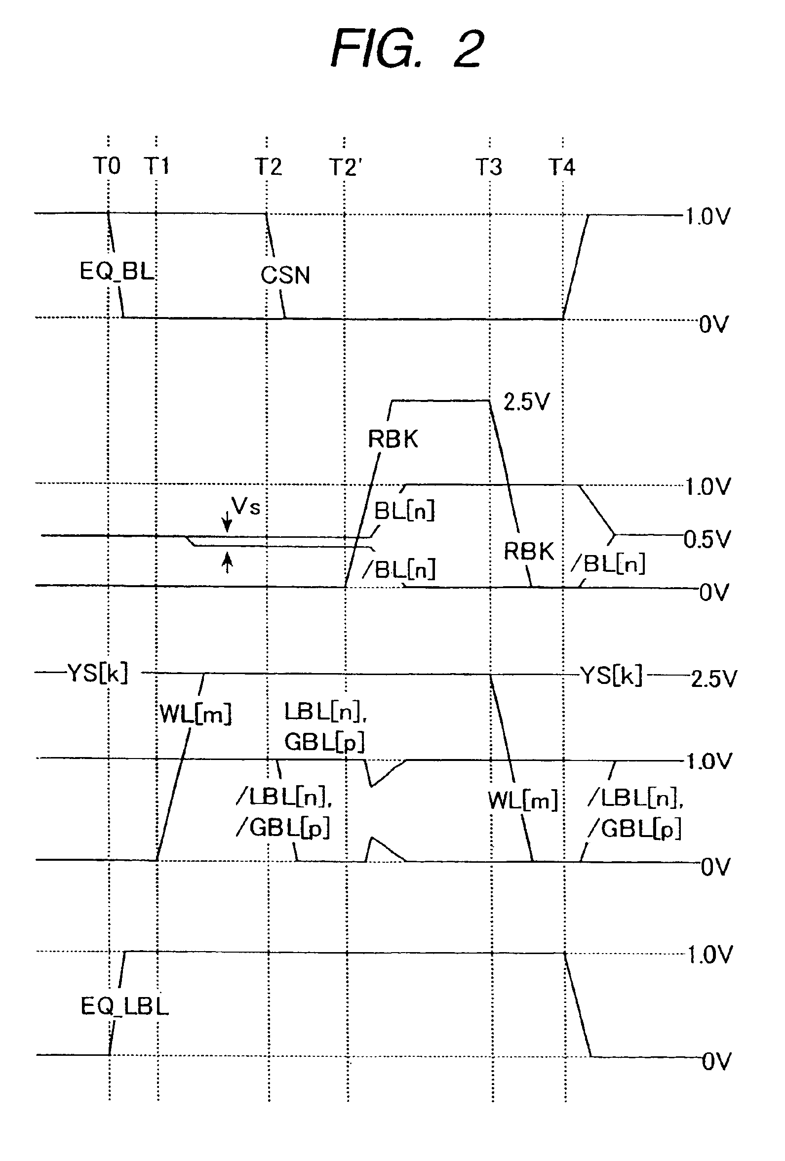
[0053]FIG. 1 shows an embodiment of a typical sensing system circuit of the present invention. C100 and M100 form a memory cell (MC). The C100 is a capacitor for storing information within the memory cell, M100 is a charge transfer NMOS transistor and VPL is a plate voltage. BL[n] and / BL[n] are bit lines, WL[m] is a word line and a memory cell is disposed at the adequate intersection to form a memory array 100. Here, the embodiment based on the folde...


PUM


Abstract

The present invention provides a sense circuit for DRAM memory cell to cover the events that a sense time becomes remarkably longer when a power source voltage is lowered, a sense time under the low voltage condition becomes shorter when temperature rises and a sense time changes to a large extent for fluctuation of processes. The present invention provides the following typical effects. A switch means is provided between the bit line BL and local bit line LBL connected to the memory cells for isolation and coupling of these bit lines. The bit line BL is precharged to the voltage of VDL / 2, while the local bit line LBL is precharged to the voltage of VDL. The VDL is the maximum amplitude voltage of the bit line BL. A sense amplifier SA comprises a first circuit including a differential MOS pair having the gate connected to the bit line BL and a second circuit connected to the local bit line LBL for full amplitude amplification and for holding the data. When the bit line BL and local bit line LBL are capacitance-coupled via a capacitor, it is recommended to use a latch type sense amplifier SA connected to the local bit line LBL.

Description

CROSS-REFERENCE TO RELATED APPLICATION[0001]This application is a continuation of Application Ser. No. 10 / 149,221 filed Jun. 10, 2002, now U.S. Pat. No. 6,687,175 which is a 371 of International Application No. PCT / JP00 / 00616 filed Feb. 4, 2000.TECHNICAL FIELD[0002]The present invention relates to a semiconductor device and particularly to a semiconductor integrated circuit device having excellent low voltage operation characteristics.BACKGROUND ART[0003]In this specification, reference is made to the following cited references identified with the reference numbers.[0004][Reference 1]“VLSI Memory Design”Kiyoo Itoh, p162;[0005][Reference 2]“Japanese Patent Laid-open No. Hei 2-24898 (corresponding U.S. Pat. No. 4,973,864);[0006][Reference 3]“Japanese Patent Laid-open No. Hei 10-3971 (corresponding U.S. Pat. No. 5,854,562);[0007][Reference 4]“1996 Symposium on VLSI Circuits Digests of Technical Papers, pp. 104-105;[0008]FIG. 26.1 of the [Reference 1] is a sensing system circuit diagram...

Claims


Application Information

Patent Timeline
Patent Type & Authority Patents(United States)
IPC IPC(8): G11C5/06G11C7/06G11C7/12G11C7/18G11C11/4091G11C11/4094G11C11/4097
CPCG11C7/04G11C7/065G11C7/08G11C7/12G11C7/18G11C11/4091G11C11/4094G11C11/4097G11C11/4076G11C2207/005G11C2207/002
Inventor MIZUNO, HIROYUKISAKATA, TAKESHIOODAIRA, NOBUHIROWATANABE, TAKAOKANNO, YUSUKE
Owner RENESAS ELECTRONICS CORP
Learn More