Signal transmitting system

a transmission system and signal technology, applied in the direction of logic circuit coupling/interface arrangement, pulse technique, instruments, etc., can solve the problems of lsi fabrication process complexity, system performance lowering, and increased system cost, so as to prevent an increase in cost and suppress timing skew

Inactive Publication Date: 2006-01-10
LONGITUDE SEMICON S A R L
View PDF5 Cites 18 Cited by
  • Summary
  • Abstract
  • Description
  • Claims
  • Application Information

AI Technical Summary

Benefits of technology

[0026]It is an object of the present invention to provide a signal transmission system which suppresses a timing skew between semiconductor integrated circuit devices that operate under different power supply voltages and also prevents an increase in the cost.
[0028]In order to reduce the number of power supplies, the values of reference voltages Vref used to determine an input voltage which are supplied to the respective semiconductor integrated circuit devices are brought into conformity with each other. Preferably, the values of the reference voltages Vref are set to 0.25 (V1+V2), making it easy to generate the reference voltages Vref. V1 and V2 represent power supply voltages VDDQ supplied to the semiconductor integrated circuit devices which send and receive signals.
[0031]In order to reduce the number of power supplies, the values of reference voltages used in the respective semiconductor integrated circuit devices are brought into conformity with each other. Preferably, the values of the reference voltages are set to 0.5V2, making it easy to generate the reference yyvoltages. V2 represents the low VDDQ.
[0034]By bringing the terminating resistor Rterm or the on resistance Ron into conformity with the characteristic impedance of the transmission line and using the ground plane shared by the semiconductor integrated circuit devices as the path of the return current flowing through the transmission line, the signal can be transmitted with good signal integrity. Furthermore, by using the same value of reference voltage in the semiconductor integrated circuit devices, the types of power supplies are reduced and the number of layers of the printed board is reduced. Since the value of an optimum reference voltage can be used at all times, the timing skew in an input circuit section is reduced.
[0035]Furthermore, inasmuch as the value of the reference voltage is set to a value that can easily be generated (e.g., 0.25 (V1+V2)), a circuit for generating the reference voltage is simple.
[0037]Consequently, there is obtained a signal transmission system which is of good signal integrity, has a reduced timing skew, and prevents cost increases.

Problems solved by technology

First, the arrangement having the voltage converter LSI as shown in FIG. 1 is problematic in that since the propagation speed of signals is reduced by the voltage converter LSI, the system performance is lowered. Furthermore, the cost of the system increases because the number of parts used is increased by using the voltage converter LSI.
The arrangement wherein the 1.5-V power supply is supplied to the 1.2-V LSI shown in FIG. 2 is problematic in that the LSI fabrication process tends to be complex because of the need for a process for making the oxide film partially thick.
Another problem is that terminals are required to supply the 1.5-V power supply, and the cost of the 1.2-V LSI is increased due to an increase in the LSI package size and the number of terminals.
Therefore, relatively expensive reference voltage generating circuits are needed, and two types of interconnection patterns for reference voltages of different potentials are required, resulting in an increased number of layers in the PCB and hence an increased system cost.
Though two types of reference voltages are required, if a reference voltage Vref that is actually supplied is limited to either one of them, then the following problem arises:
However, when the input signal goes low, the input circuit (receiver) responds more slowly than when the reference voltage Vref of 0.71 V is supplied, resulting in a timing skew in the input circuit.
If the timing skew increases due to a reduction in the reference voltage Vref, then the possibility of an error becomes higher.
As there is a possibility for an increased number of PCB layers, the system cost tends to rise.
Though there are two types of reference voltages and terminating voltages VTT, if a reference voltage Vref and a terminating voltage VTT that are actually supplied are limited to either one of them, then the same problem as with FIG. 5 arises.

Method used


Image

  • Signal transmitting system
  • Signal transmitting system
  • Signal transmitting system

Examples


first embodiment

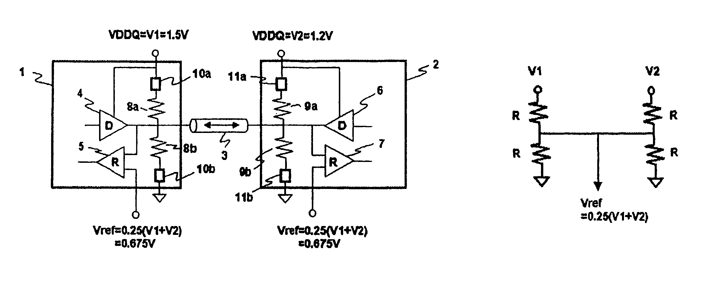
[0098]FIG. 10 is a circuit diagram of an arrangement of a signal transmission system according to the present invention.

[0099]FIG. 10 shows a specific example of the signal transmission system according to the first working example, for sending and receiving a single-ended signal. FIG. 10(a) shows an equivalent circuit for sending a signal from 1.5-V LSI 1 to 1.2-V LSI 2, and FIG. 10(b) shows an equivalent circuit for sending a signal from 1.2-V LSI 2 to 1.5-V LSI 1.

[0100]In FIG. 10, switches that are turned off, receivers, and drivers that are set to a high impedance state on the signal reception side that do not contribute to the values of potentials, are omitted from the illustration, and the resistances of switches that are turned on, are included in the values of resistors 8a, 8b, 9a and 9b.

[0101]The driver for sending a signal comprises a pMOS and an nMOS transistors which are push-pull-connected. Bidirectional bus 3 which is a transmission line has a characteristic impedance...

second embodiment

[0122]FIG. 13 is a circuit diagram of an arrangement of a signal transmission system according to the present invention. FIG. 13 shows a specific example of the signal transmission system according to the first working example, for sending and receiving a single-ended signal. FIG. 13(a) shows an equivalent circuit for sending a signal from 1.5-V LSI 1 to 1.2-V LSI 2, and FIG. 13(b) shows an equivalent circuit for sending a signal from 1.2-V LSI 2 to 1.5-V LSI 1.

[0123]In FIG. 13, switches that are turned off, receivers, and drivers that are set to a high impedance state on the signal reception side that do not contribute to the values of potentials, are omitted from the illustration, and the resistances of switches that are turned on, are included in the values of resistors 8a, 8b, 9a and 9b.

[0124]The driver for sending a signal comprises a pMOS and an nMOS transistors which are push-pull-connected. Bidirectional bus 3 which is a transmission line has a characteristic impedance Z0 o...

third embodiment

[0141]FIG. 15 is a circuit diagram of an arrangement of a signal transmission system according to the present invention. FIG. 15 shows a specific example of the signal transmission system according to the first working example, for sending and receiving a single-ended signal. FIG. 15(a) shows an equivalent circuit for sending a signal from 1.5-V LSI 1 to 1.2-V LSI 2, and FIG. 15(b) shows an equivalent circuit for sending a signal from 1.2-V LSI 2 to 1.5-V LSI 1.

[0142]In FIG. 15, switches that are turned off, receivers, and drivers that are set to a high impedance state on the signal reception side that do not contribute to the values of potentials, are omitted from the illustration, and the resistances of switches that are turned on, are included in the values of resistors 8a, 8b, 9a and 9b.

[0143]The driver for sending a signal comprises a pMOS and an nMOS transistors which are push-pull-connected. Bidirectional bus 3 which is a transmission line has a characteristic impedance Z0 o...


PUM


Abstract

Semiconductor integrated circuit devices that operate under different power supply voltages are directly interconnected by a bidirectional bus which is a transmission line. A driver is of a push-pull type and a reception side is CTT-terminated. If a terminating resistor is in conformity with the characteristic impedance of the transmission line, the on resistance of the driver is equal to or lower than the characteristic impedance. If the on resistance of the driver is in conformity with the characteristic impedance of the transmission line, the value of the terminating resistor is equal to or lower than the characteristic impedance of the transmission line. If the reception side is VTT-terminated, the value of the VTT is ½ of a lower one of power supply voltages that are supplied to the respective semiconductor integrated circuit devices. The value of the terminating resistor is in conformity with the characteristic impedance of the transmission line. The semiconductor integrated circuit devices use a common reference voltage for determining the signal voltage.

Description

BACKGROUND OF THE INVENTION[0001]1. Field of the Invention[0002]The present invention relates to a signal transmission system for transmitting a signal between a plurality of semiconductor integrated circuit devices that operate under different power supply voltages.[0003]2. Description of the Related Art[0004]There has heretofore been a system which is required to transmit a signal between semiconductor integrated circuit devices that operate under different power supply voltages. FIG. 1 shows a conventional arrangement of such a system. The system shown in FIG. 1 transmits a single-ended signal between a 1.8-V semiconductor integrated circuit device (LSI 1) and a 1.5-V semiconductor integrated circuit device (LSI 3). A voltage converter LSI (LSI 2) for converting voltages is provided between the 1.8-V semiconductor integrated circuit device and the 1.5-V semiconductor integrated circuit device for relaying a signal to be sent and received between LSI 1 and LSI 3. LSI 1 and LSI 2 a...

Claims


Application Information

Patent Timeline
IPC IPC(8): H03K17/16H03K19/0175G11C7/10
CPCG11C7/1006H04L25/0278H04L5/16
Inventor NISHIO, YOJIFUNABA, SEIJI
Owner LONGITUDE SEMICON S A R L
Why Eureka
Try Eureka