
Magneto-optical switching backplane for processor interconnection

a backplane and processor technology, applied in the direction of optical elements, multiplex communication, instruments, etc., can solve the problems of limiting the maximum achievable bandwidth, communication between processor chips, and reaching the limits of interconnections between chips or between multi-chip modules

Inactive Publication Date: 2006-01-03
IBM CORP
View PDF5 Cites 27 Cited by
  • Summary
  • Abstract
  • Description
  • Claims
  • Application Information

AI Technical Summary

Benefits of technology

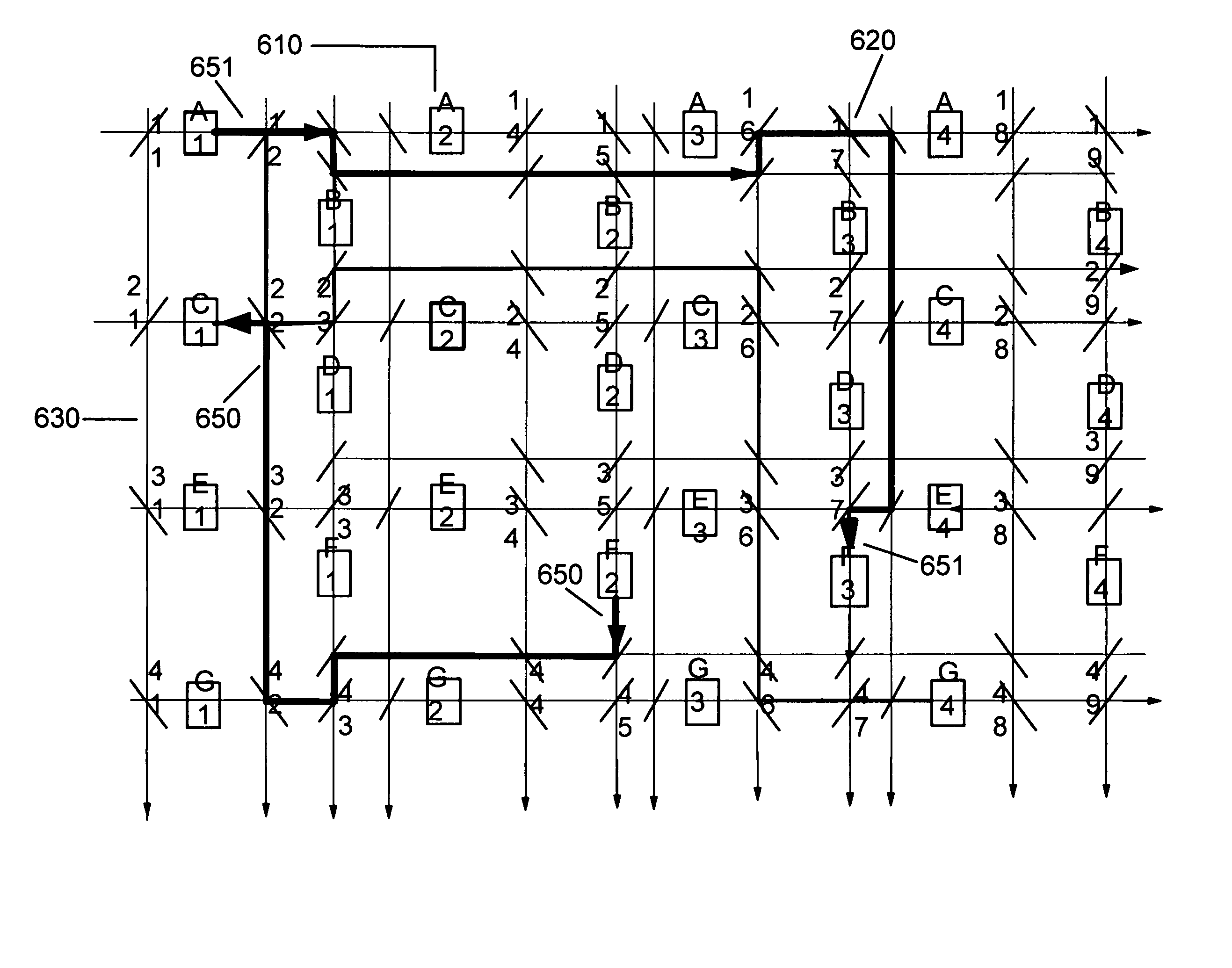
[0008]It is yet a further object of the invention to provide for the whole optical interconnection network, based on planar, ridge, or cylindrical waveguides. Such waveguide types are well known in the appropriate arts. Also, for providing apparatus and method for controlling the routers in such an optical network. The routers allow establi

Problems solved by technology

A major packaging challenge of computing systems always has been the communication infrastructure, the so called wiring backplane of sufficient bandwidth.
However, as data rates increase metal interconnects between chips, or between multi chip modules, are reaching their limits.
Communication between processor chips is starting to be a performance bottleneck.
Metal interconnects suffer from loss, cross talk, excessive power requirements, all limiting the maximum achievable bandwidth.
As a result of such difficulties optical interconnections are now being seriously considered to take the place of metal wiring.
However, the actualization of a purely optical backplane hitherto faced formidable obstacles.
There are problems with the integration of lasers, detectors, and waveguides into necessarily small spaces afforded in microprocessor technology.
There is also the problem of how to direct light pulses along an optical network at GHz speeds.
Then, there is the problem of process integration, namely the difficulty of the processing technology needed to incorporate lasers, detectors, and waveguides into a CMOS technology framework.

Method used


Image

  • Magneto-optical switching backplane for processor interconnection
  • Magneto-optical switching backplane for processor interconnection
  • Magneto-optical switching backplane for processor interconnection

Examples


Embodiment Construction

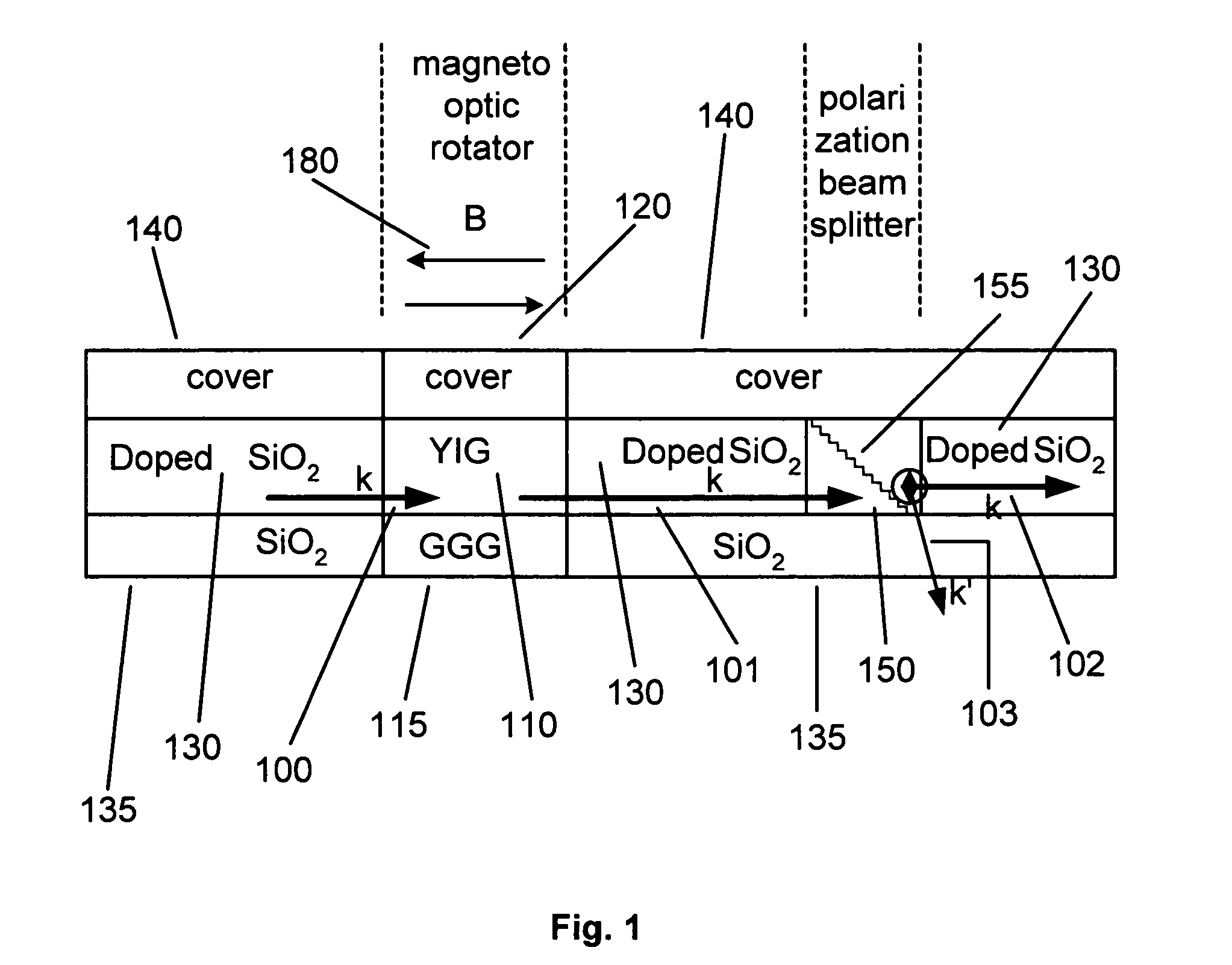
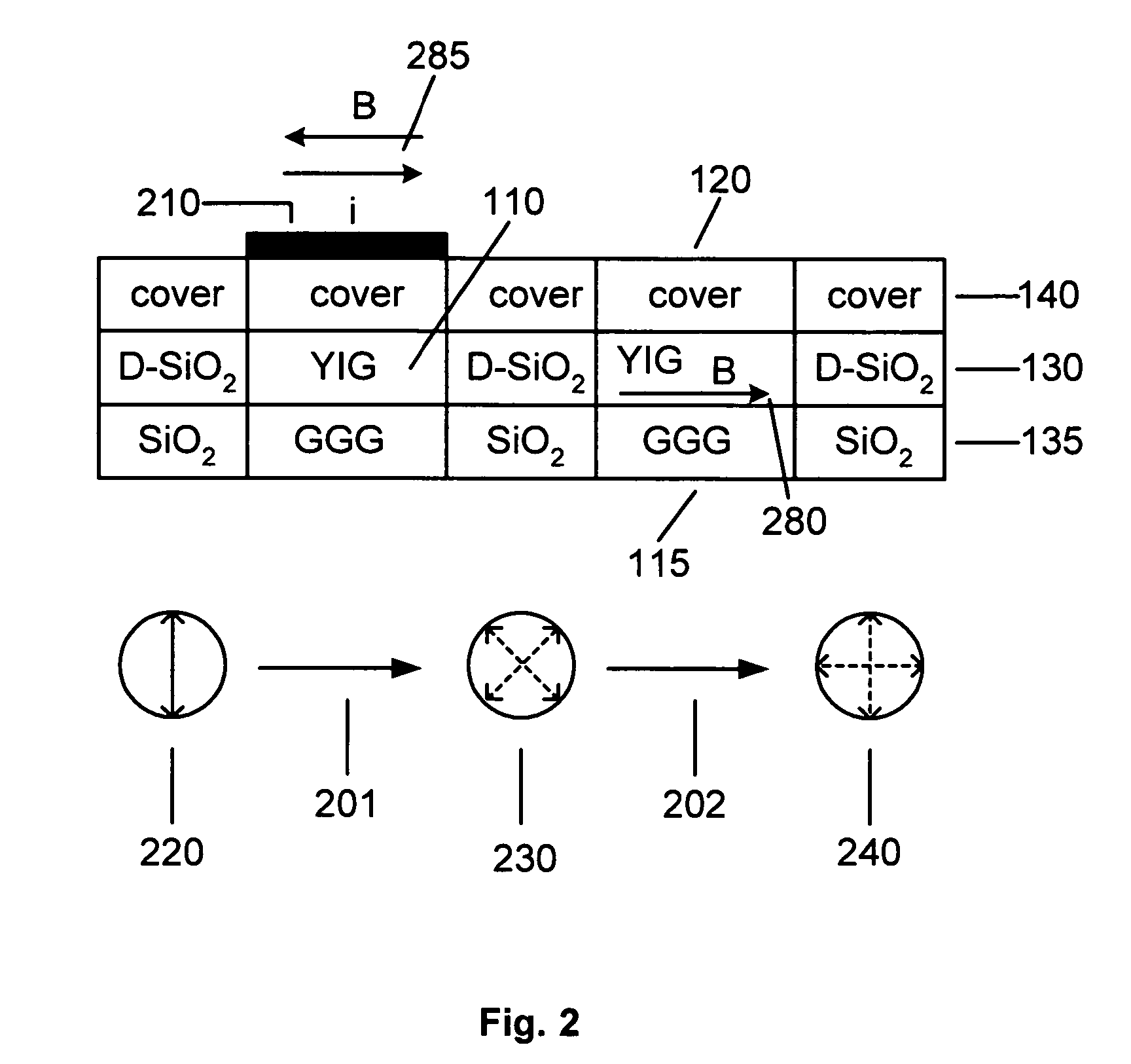
[0018]FIG. 1 shows elements of a router for polarized light. The router comprise of two parts, a magneto optic rotator (MOR) followed by a polarization beam splitter (PBS). In one embodiment these two parts of the router are seamlessly integrated into an optical waveguide. FIG. 1 shows a sandwich structure for both the router and for the shown pieces of the waveguide network. The waveguide network of the optical backplane is based on a SiO2, or alternatively a polymer, waveguide structure. In one embodiment an undoped SiO2 optical layer 135 of an index of refraction (ns) is interfacing with a doped SiO2 layer 130. Due to the doping, the doped SiO2 has an index of refraction, (nf) approximately equal to 1.45. The waveguide typically needs a doped SiO2 which interfaces, that is, it is deposited on the top, or below, of an undoped SiO2. The requirement of this undoped SiO2 layer is for it to have a lower refractive index than the doped SiO2 layer. In the embodiment of a sandwich struct...


PUM


Abstract

A system and method are disclosed for an optical backplane in an electronic processor that comprises of a plurality of processing units. The backplane is comprising of a network of optical waveguides which can guide polarized light. Furthermore, the backplane has magneto optic routers for steering light at the vertexes of the network, and the backplane also has optical devices for operationally connecting the processing units to the network. The backplane network affords an optical interconnection amongst all of the processing units.

Description

CROSS REFERENCE TO A RELATED APPLICATION[0001]This application is a division of application Ser. No. 10 / 073,450, filed Feb. 11, 2002, now U.S. Pat. No. 6,816,637.FIELD OF THE INVENTION[0002]This invention relates to a system, and a method, for using an optical backplane to provide ultra high frequency optical interconnections amongst microprocessors. The backplane is comprised of an optical waveguide network and magneto-optical routers.BACKGROUND OF THE INVENTION[0003]Th speed of computing devices, such as electronic processors, has been steadily increasing. Processing speed is accompanied by a need for rapid communication amongst processing units. The communication bandwidth requirements of microprocessors (the words processing unit and microprocessor will be used interchangeably) are roughly proportional with speed, and chip cycle times are reaching into the GHz domain. The central computing complexes of large computers comprise of many individual microprocessors, packaged into mu...

Claims


Application Information

Patent Timeline
IPC IPC(8): G02B6/35G02B6/28G02F1/295G02B6/26G02B6/43
CPCG02B6/43G02B6/2848G02B6/2746
Inventor MCGLASHAN-POWELL, MAURICEHOBBS, PHILIP CHARLES DANBY
Owner IBM CORP
Learn More