Method of forming miniaturized polycrystalline silicon gate electrodes using selective oxidation

a polycrystalline silicon and gate electrode technology, applied in the direction of semiconductor devices, electrical devices, transistors, etc., can solve the problems of increasing the disadvantage of gate electrodes, reducing the accuracy of gate electrodes, so as to reduce the fringing capacitance, less demanding photolithographic capabilities, and preserving the effect of device performan

Inactive Publication Date: 2005-12-27
GLOBALFOUNDRIES INC
View PDF4 Cites 9 Cited by
  • Summary
  • Abstract
  • Description
  • Claims
  • Application Information

AI Technical Summary

Benefits of technology

[0004]An advantage of the present invention is a method of manufacturing a semiconductor device comprising a transistor having a miniaturized gate electrode with reduced fringing capacitance.
[0005]Another advantage of the present invention is a method of fabricating a semiconductor device comprising a transistor having an accurately dimensioned gate electrode with a height less than 1,000 Å and a width less than 500 Å, without adversely impacting gate dielectric integrity and transistor reliability while preserving the advantageous device performance associated with deep source / drain implants required for good contacts.
[0006]Another advantage of the present invention is a method of fabricating a semiconductor device comprising transistors having a gate electrode width less than 500 Å and a height less than 1,000 Å with significantly less demanding photolithographic capabilities which would otherwise be required for such small gates.
[0007]Additional advantages and other features of the present invention will be set forth in the description which follows, and in part will become apparent to those having ordinary skill in the art upon examination of the following or may be learned by practice of the present invention. The advantages of the present invention may be realized and obtained as particularly pointed out in the appended claims.
[0008]According to the present invention, the foregoing and other advantages are achieved in part by a method of manufacturing a semiconductor device, the method comprising: forming a polysilicon gate electrode precursor having first side surfaces at a first width and a first upper surface at a first height, over a main surface of the semiconductor substrate with a gate insulating layer therebetween; selectively oxidizing the first side surfaces and first upper surface of the polysilicon gate electrode precursor to form oxidized layers thereon; and removing the oxidized layers from the polysilicon gate electrode precursor to form a polysilicon gate electrode having second side surfaces at a second width less than the first width and a second upper surface at a second height less than the first height.
[0009]Embodiments of the present invention comprise ion implanting impurities, using the polysilicon gate electrode precursor as a mask, to form deep source / drain regions; forming nitride layers on the main surface of the semiconductor substrate over the deep source / drain layers on opposite sides of the polysilicon gate electrode precursor; selectively oxidizing the first side surfaces and first upper surface of the polysilicon gate electrode precursor to form the oxidized layers thereon, removing the oxidized layers from the polysilicon gate electrode precursor to form the polysilicon gate electrode, removing the nitride layers, and ion implanting impurities, using the polysilicon gate electrode as a mask, to form source / drain extensions. Embodiments of the present invention further include forming dielectric sidewall spacers on the second side surfaces of the polysilicon gate electrode and forming metal silicide layers on the second upper surface of the polysilicon gate electrode and on the main surface of the semiconductor substrate over the deep source / drain regions. Embodiments of the present invention enable formation of polysilicon gate electrodes having a height less than 1,000 Å, such as 300 Å to 900 Å, and a width less than 500 Å, such as 150 Å to 400 Å.

Problems solved by technology

As the drive for faster miniaturized semiconductor devices proceeds apace, it becomes increasingly more difficult to fabricate device features without engendering disadvantages.
It is particularly challenging to form gate electrodes having a reduced height and a reduced width, such as a height less than 1,000 Å and a width less than 500 Å, without creating various issues.
For example, it is extremely difficult to pattern a gate electrode having a width less than 500 Å by conventional photolithographic techniques with any degree of precision and reproducibility.
Moreover, as the gate width decreases, the aspect ratio of the gate electrode disadvantageously increases.
However, the gate electrode must be sufficient high to prevent impurity ion penetration therethrough into the underlying gate dielectric layer with an attendant decrease in reliability, as during ion implantation to form deep source / drain regions.
Moreover, a high gate height contributes to fringing capacitance between the gate electrode and associated source / drain regions.

Method used


Image

  • Method of forming miniaturized polycrystalline silicon gate electrodes using selective oxidation
  • Method of forming miniaturized polycrystalline silicon gate electrodes using selective oxidation
  • Method of forming miniaturized polycrystalline silicon gate electrodes using selective oxidation

Examples


Embodiment Construction

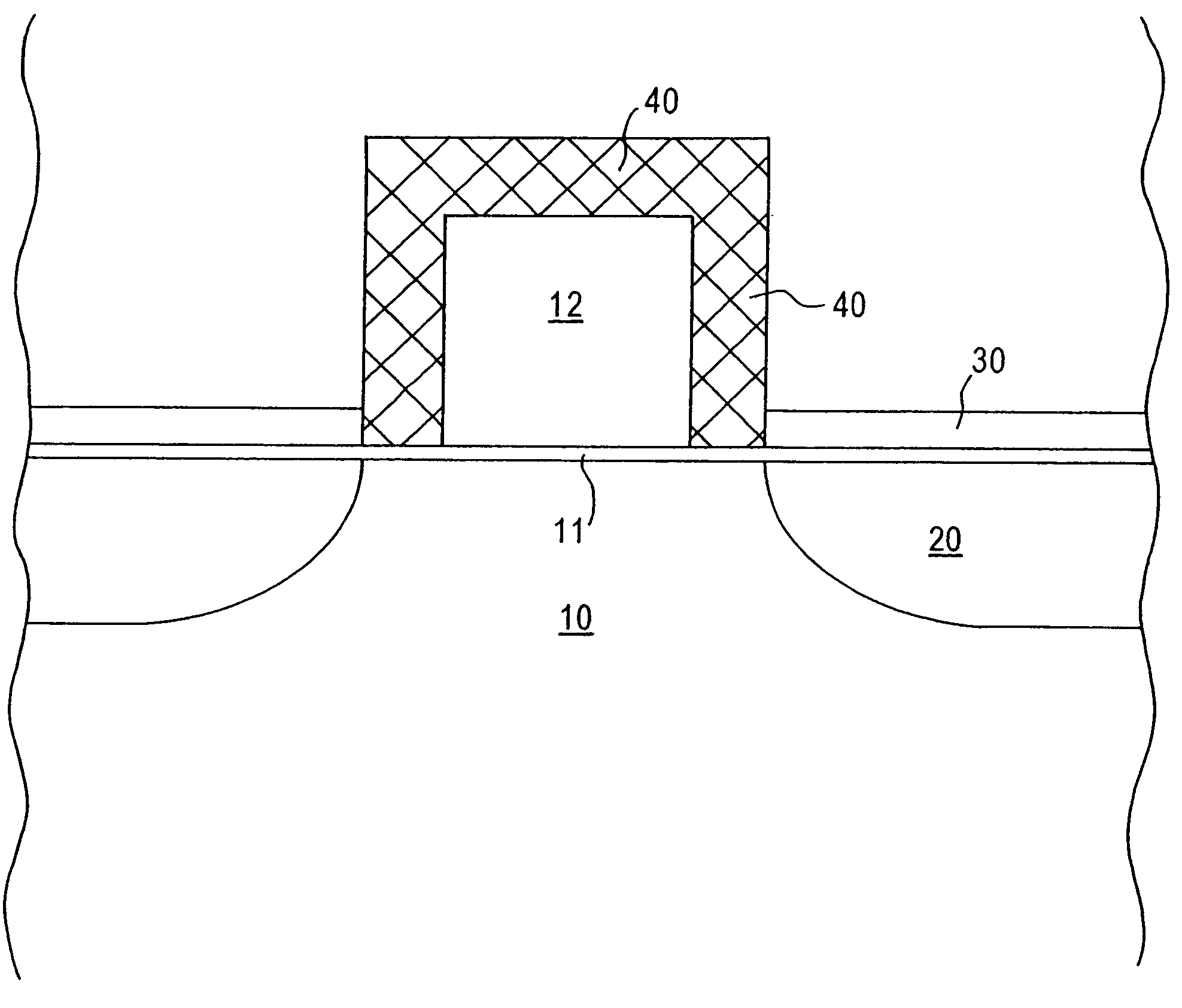
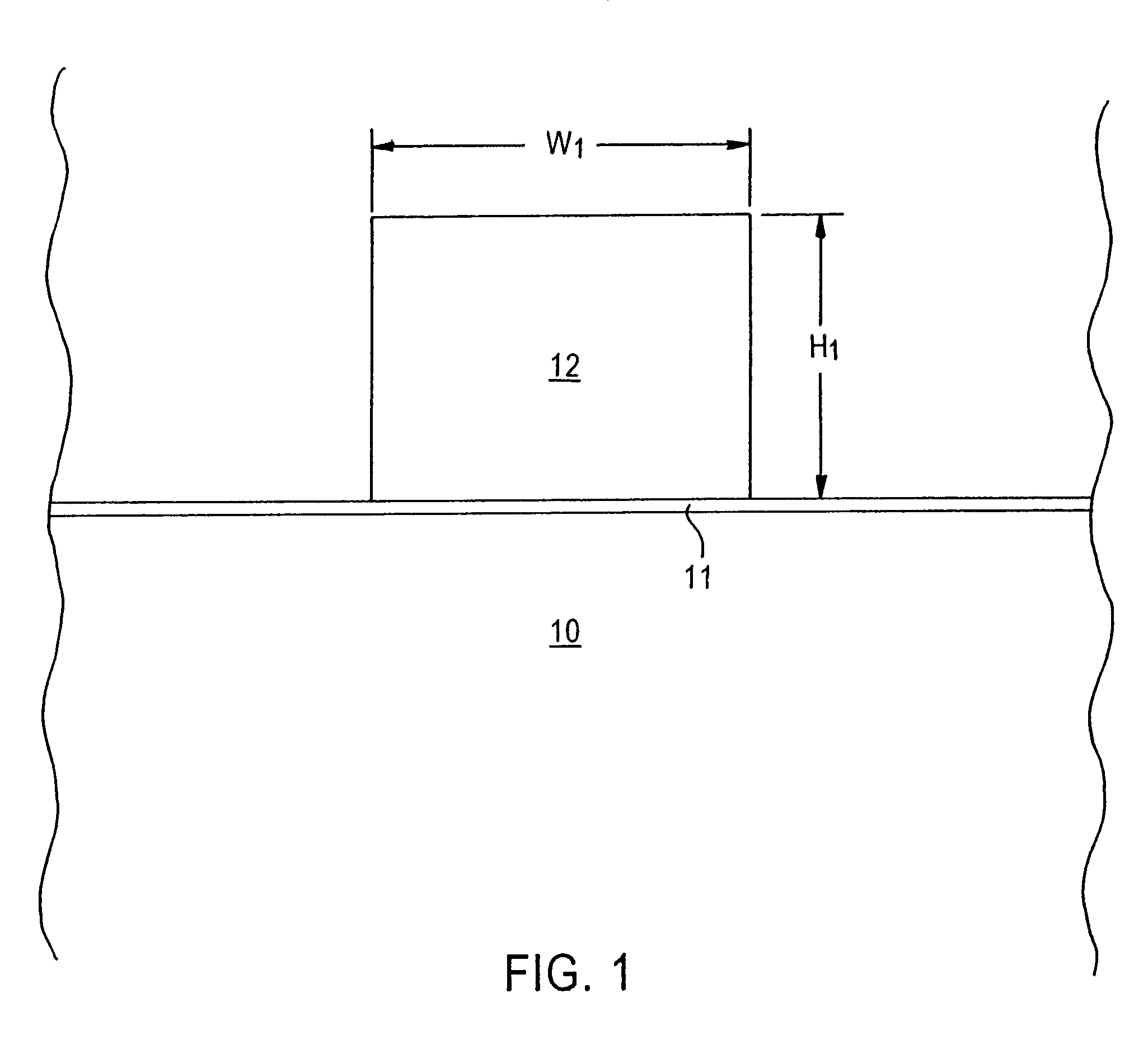
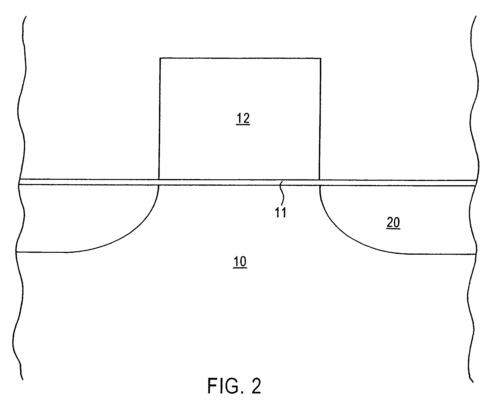
[0012]The present invention addresses and solves problems attendant upon fabricating miniaturized semiconductor devices, particularly transistors having a miniaturized gate electrode, such as a gate electrode with a height less than 1,000 Å and a width less than 500 Å. Conventional photolithographic techniques are limited in their ability resolution capabilities and, hence, cannot be used to pattern gate electrodes with a width less than 500 Å with the requisite precision and reproducibility. Reduction of the gate width disadvantageously increases the aspect ratio of the gate electrode. However, the gate electrode must be sufficiently high to prevent implanted impurities from penetrating therethough into the underlying gate oxide layer with attendant degradation thereof, as during ion implantation to form deep source / drain regions.

[0013]The present invention addresses and solves such problems by forming a gate electrode precursor having a first width fully within the resolution capa...


PUM


Abstract

Ultra narrow and thin polycrystalline silicon gate electrodes are formed by patterning a polysilicon gate precursor, reducing its width and height by selectively oxidizing its upper and side surfaces, and then removing the oxidized surfaces. Embodiments include patterning the polysilicon gate precursor with an oxide layer thereunder, ion implanting to form deep source / drain regions, forming a nitride layer on the substrate surface on each side of the polysilicon gate precursor, thermally oxidizing the upper and side surfaces of the polysilicon gate precursor thereby consuming silicon, and then removing the oxidized upper and side surfaces leaving a polysilicon gate electrode with a reduced width and a reduced height. Subsequent processing includes forming shallow source / drain extensions, forming dielectric sidewall spacers on the polysilicon gate electrode and then forming metal silicide layers on the upper surface of the polysilicon gate electrode and over the source / drain regions.

Description

TECHNICAL FIELD[0001]The present invention relates to the fabrication of miniaturized semiconductor devices comprising transistors with a gate electrode having a significantly reduced height and width. The present invention is particularly applicable to ultra large scale integrated circuit systems having features in the deep sub-micron regime.BACKGROUND ART[0002]As the drive for faster miniaturized semiconductor devices proceeds apace, it becomes increasingly more difficult to fabricate device features without engendering disadvantages. It is particularly challenging to form gate electrodes having a reduced height and a reduced width, such as a height less than 1,000 Å and a width less than 500 Å, without creating various issues. For example, it is extremely difficult to pattern a gate electrode having a width less than 500 Å by conventional photolithographic techniques with any degree of precision and reproducibility. Moreover, as the gate width decreases, the aspect ratio of the g...

Claims


Application Information

Patent Timeline
Patent Type & Authority Patents(United States)
IPC IPC(8): H01L21/28H01L21/3205H01L21/336H01L29/78
CPCH01L21/28035H01L21/28123H01L29/6653H01L29/6659H01L29/665H01L29/6656H01L29/7833Y10S438/976
Inventor SULTAN, AKIFXIANG, QIYU, BIN
Owner GLOBALFOUNDRIES INC
Why Eureka
Try Eureka