
Pixel modulation apparatus and method thereof

a modulation apparatus and pixel technology, applied in signal generators with optical-mechanical scanning, color televisions with bandwidth reduction, television systems, etc., can solve the problems of deteriorating printing quality, high cost of pixel modulation circuits for video, and inability to secure predetermined video image quality, etc., to achieve accurate change the quantity of laser light, low cost, and easy generation

Inactive Publication Date: 2005-11-08
CANON KK
View PDF6 Cites 2 Cited by
  • Summary
  • Abstract
  • Description
  • Claims
  • Application Information

AI Technical Summary

Benefits of technology

[0018]In view of the back ground mentioned above, an object of the present invention is to provide a pixel modulation apparatus that can easily generate a laser control signal suitable for various images such as gradated images and character images and can accurately change the quantity of laser light and further can be constructed by, for example, a pure CMOS process and still further is low in cost, and a method thereof.

Problems solved by technology

However, the digital pixel modulation and the analog pixel modulation, which are used in the conventional image forming apparatus, have the following problems.
For such input images, the conventional digital pixel modulation could not secure sufficient number of pixel divisions, and thereby, a predetermined video image quality could not be secured.
Consequently, a pixel modulation circuit for video has been expensive.
Consequently, the desired control of the light emission of laser diodes could not performed in the conventional digital image modulation, and thereby the quality of printing has been deteriorated.

Method used


Image

  • Pixel modulation apparatus and method thereof
  • Pixel modulation apparatus and method thereof
  • Pixel modulation apparatus and method thereof

Examples


Embodiment Construction

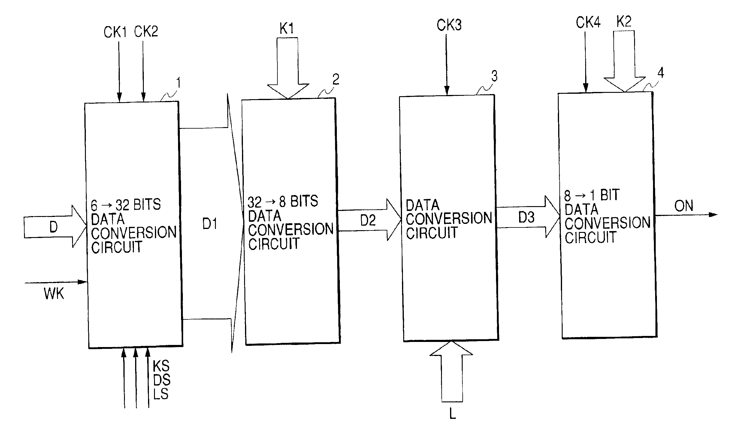
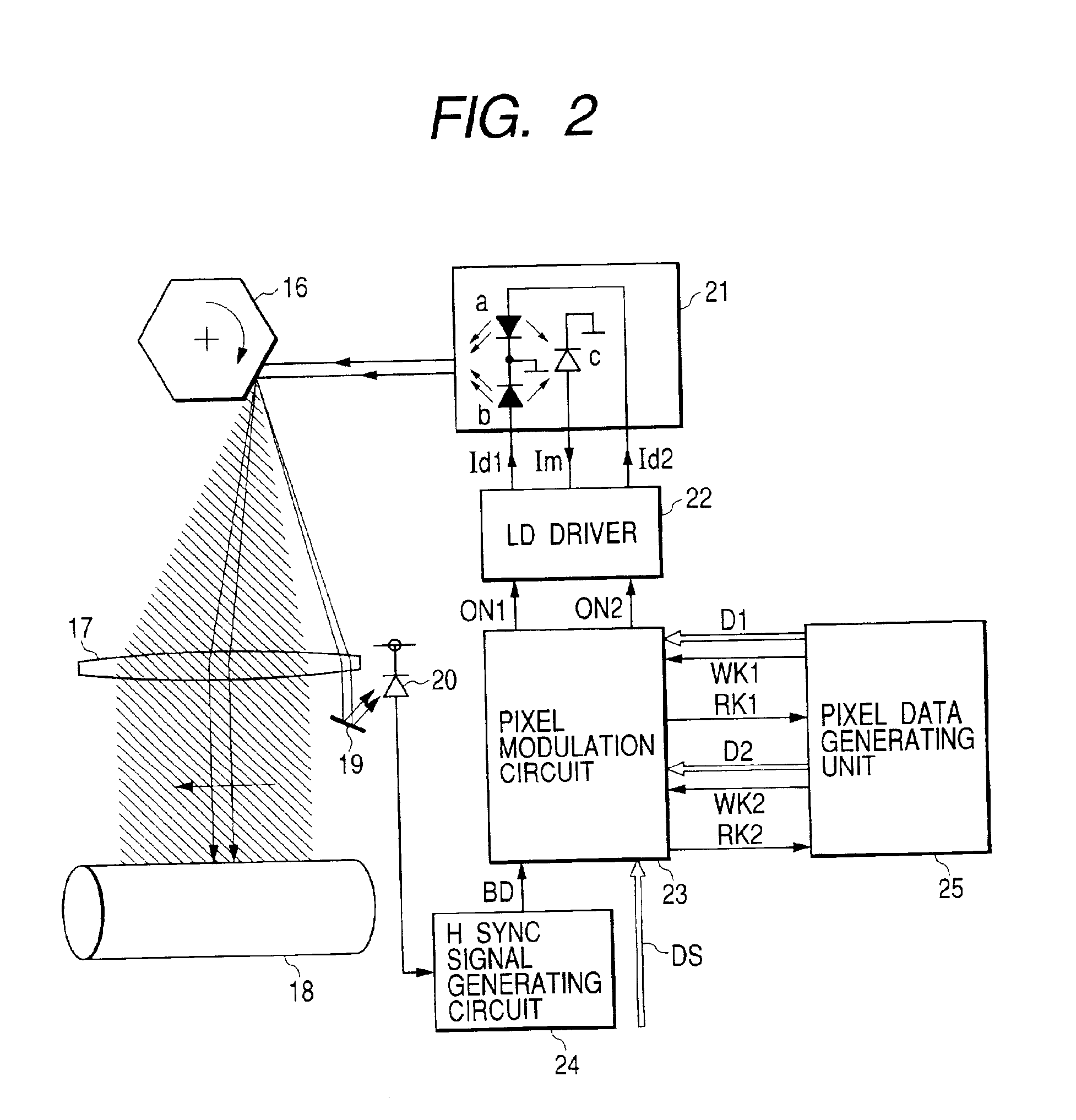
[0041]FIG. 5 shows a pixel modulation circuit according to the present invention applied to a color printer using four color pieces of toner of yellow (Y), cyan (Cy), magenta (Mg) and black (Bk). The pixel modulation circuit is composed of four data conversion circuits 1-4. The pixel modulation circuit is provided for each laser beam. The other configuration of the image writing portion provided with the pixel modulation circuit is the same as that shown in FIG. 2.

Description of Data Conversion Circuit 1

[0042]Each of pixel data D (composed of six bits in this case) generated by picking up an object image with a scanner or the like and a write clock WK are input into a 6-to-32-bit data conversion circuit 1 for converting 6 bit data to 32 bit data. Then, the pixel data D are converted to 32 bit data D1.

[0043]The 6-to-32-bit data conversion circuit 1 is, for example, a 64-word random access memory (RAM). One word is composed of 32 bits. The pixel data D are input to the address lines o...


PUM


Abstract

A pixel modulation apparatus for converting pixel data D composed of N1 bits to a pixel data signal composed of one bit. The pixel data D is input into the apparatus at a pixel period T0. The apparatus includes a first data conversion unit which converts the pixel data D to pixel data D1 expanded to N2 bits (N2>N1) at the period T0, a second data conversion unit which converts the pixel data D1 to pixel data D2 composed of N3 / m bits at a period T0 / m, a third data conversion unit which inputs n data from among the pixel data D2 and pixel data Dd2 constituting the pixel data D2 before having the period T0 / m to execute logical sum operations a predetermined number (equal to or less than n) of times to convert the n data to pixel data D3 composed of N3 bits, including additional data corresponding to the predetermined number, and a fourth data conversion unit which converts the pixel data D3 to the pixel data signal composed of one bit at the period T0 / m.

Description

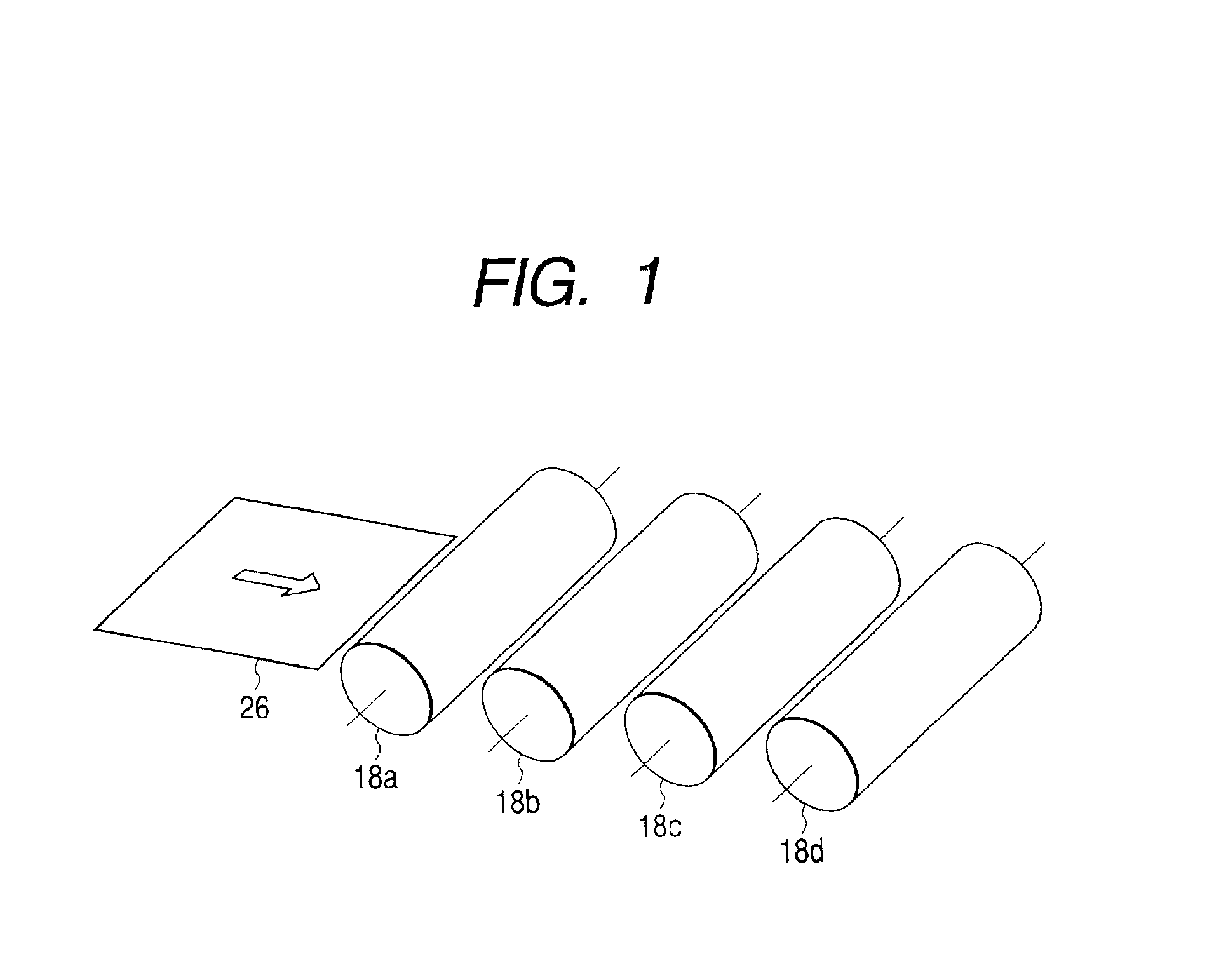
BACKGROUND OF THE INVENTION[0001]1. Field of the Invention[0002]The present invention relates to a pixel modulation apparatus and a method thereof, and more particularly to a pixel modulation apparatus capable of performing high-accuracy pulse width modulation for controlling the light emission of a laser on a pixel basis in an image forming apparatus which uses the laser to form an image, and a method of such pixel modulation.[0003]2. Related Background Art[0004]An image forming apparatus using a laser beam has been used as one of apparatus performing the control of the quantity of a laser beam by means of a pulse width modulation. As for such an image forming apparatus, first, a color image forming apparatus is simply described as an example thereof.[0005]A color image forming process of such an color image forming apparatus generally uses four kinds of toners of yellow (Y), cyan (C), magenta (Mg) and black (Bk) severally. Such a color image forming process takes a time four times...

Claims


Application Information

Patent Timeline
IPC IPC(8): H04N1/405B41J2/44H04N1/113H04N1/23
CPCH04N1/4056
Inventor KAWASAKI, SOMEIISEKI, MASAMIMARU, HIROYUKIKAWANO, FUJIO
Owner CANON KK
Learn More