
Single and double-gate pseudo-FET devices for semiconductor materials evaluation

a single-gate, semiconductor material technology, applied in individual semiconductor device testing, semiconductor/solid-state device testing/measurement, instruments, etc., can solve the problems of difficult use of hgfet, inability inability to use hgfet to detect light or use light, etc., to achieve fast turn-around techniques, minimize parasitic resistance, and achieve electrical properties.

Inactive Publication Date: 2005-10-18
INT BUSINESS MASCH CORP
View PDF4 Cites 8 Cited by
  • Summary
  • Abstract
  • Description
  • Claims
  • Application Information

AI Technical Summary

Benefits of technology

Enables fast and convenient evaluation of electrical properties in SOI materials regardless of Si thickness, temperature, and layer structure, including multi-layer structures, with reduced impedance and the ability to detect light, overcoming the limitations of traditional HgFET methods.

Problems solved by technology

However, the mercury-based pseudoFET (HgFET) becomes difficult to use as the thickness of the Si layer is reduced below several hundred Angstroms because the threshold voltage of the HgFET can become comparable to the breakdown voltage of the underlying BOX.
It also is not useful for multi-layer structures such as strained silicon on silicon / germanium on oxide where the electrical properties of the two layers act in parallel and the HgFET cannot separate them.
The HgFET cannot be used to detect light or to use light as a further evaluation technique because it is virtually always used in an upside down configuration due to the liquid mercury electrodes and therefore is in the dark.

Method used


Image

  • Single and double-gate pseudo-FET devices for semiconductor materials evaluation
  • Single and double-gate pseudo-FET devices for semiconductor materials evaluation
  • Single and double-gate pseudo-FET devices for semiconductor materials evaluation

Examples


Embodiment Construction

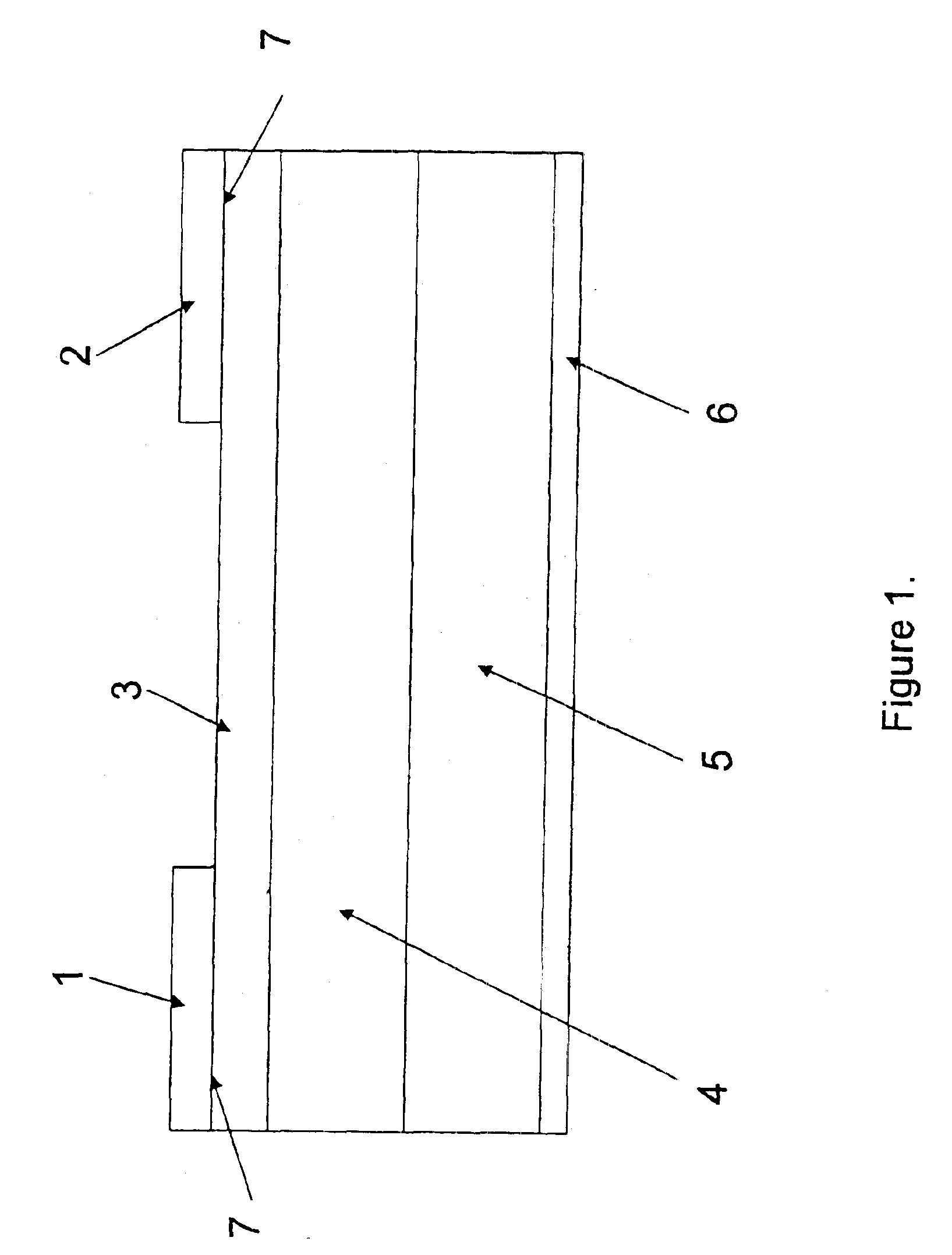
[0023]FIG. 1 shows a cross section of a single gate pseudo FET device. Silicon layer 3 resides on a buried oxide insulator 4 which resides on a Si bulk region 5. The bottom of the FET is contacted with metal 6 such as sputtered Au, Al, Cu, Cr, or other metal to provide a wide area bottom contact. (However, pseudoFET devices have been known to function satisfactorily without a bottom metal layer when the doping level and device area are sufficiently large.) Source electrode 1 and drain electrode 2 are made with Al, Er, Gd, Nd, Ti or Y, covered by Ag, Al, Au, Cr, Cu, Mg, Ni or Pt in order to provide an ohmic contact to electrons at interface 7 between the Si and electrode. Electrodes 1 and 2 may also be made with Au, Ag, Pt, Al, or Mg with or without additional covering metal to provide ohmic contact to holes at interface 7. The metal electrodes 1, 2, and 6 may be provided by evaporation or sputtering, for example. The device may be rectangular, circular, or another geometric shape. L...


PUM


Abstract

Several methods and structures are disclosed for determining electrical properties of silicon-on-insulator (SOI) wafers and alternate versions of such wafers such as strained silicon:silicon / germanium:-on-insulator (SSGOI) wafers. The analyzed electrical properties include mobilities, interface state densities, and oxide charge by depositing electrodes on the wafer surface and measuring the current-voltage behavior using these electrodes. In a single gate structure, the source and drain electrodes reside on the wafer surface and the buried insulator acts as the gate oxide, with the substrate acting as the gate electrode. In a double gate structure, an oxide is used on the upper surface between the source and drain electrodes and an additional metal layer is used on top of this oxide to act as a second gate electrode. Light of broad spectrum or specific wavelength may be used to alter electrical carrier densities in the region between the electrodes to further analyze the electrical properties of the material, or alternatively, the device can be used as a detector of light having a wavelength shorter than the bandgap wavelength of the Si surface.

Description

BACKGROUND[0001]1. Field of the Invention[0002]The present invention is directed to a method of determining electrical properties of silicon-on-insulator (SOI) wafers and alternate versions of such wafers such as strained silicon:silicon / germanium:-on-insulator (SSGOI) wafers. More specifically, the subject invention analyzes electrical properties of such SOI wafers such as mobilities, interface state densities, and oxide charge by depositing electrodes on the wafer surface and measuring the current-voltage behavior using these electrodes. In a single gate structure, the source and drain electrodes reside on the wafer surface and the buried insulator acts as the gate oxide, with the substrate acting as the gate electrode. In a double gate structure, an oxide is used on the upper surface between the source and drain electrodes and an additional metal layer is used on top of this oxide to act as a second gate electrode. Light of broad spectrum or specific wavelength may be used to alt...

Claims


Application Information

Patent Timeline
Patent Type & Authority Patents(United States)
IPC IPC(8): H01L21/336H01L29/786H01L29/417H01L29/40H01L29/66H01L21/02H01L23/544H01L29/45H01L29/423G01R31/26H01L31/08
CPCH01L21/28512H01L22/14H01L22/34H01L29/41733H01L29/42384H01L29/458H01L29/66742H01L29/66772H01L29/78645H01L29/78648H01L29/78654H01L29/78687H01L31/08G01R31/2648H01L21/84H01L2924/3011
Inventor HOVEL, HAROLD J.MCKOY, THERMON E.
Owner INT BUSINESS MASCH CORP
Learn More