Electro-optical-device driving method, image processing circuit, electronic apparatus, and correction-data generating method
a technology of optical devices and driving methods, applied in the direction of static indicating devices, instruments, television systems, etc., can solve problems such as uneven display of images, and achieve the effect of enhancing the quality of displayed images
- Summary
- Abstract
- Description
- Claims
- Application Information
AI Technical Summary
Benefits of technology
Problems solved by technology
Method used
Image

Examples
first embodiment
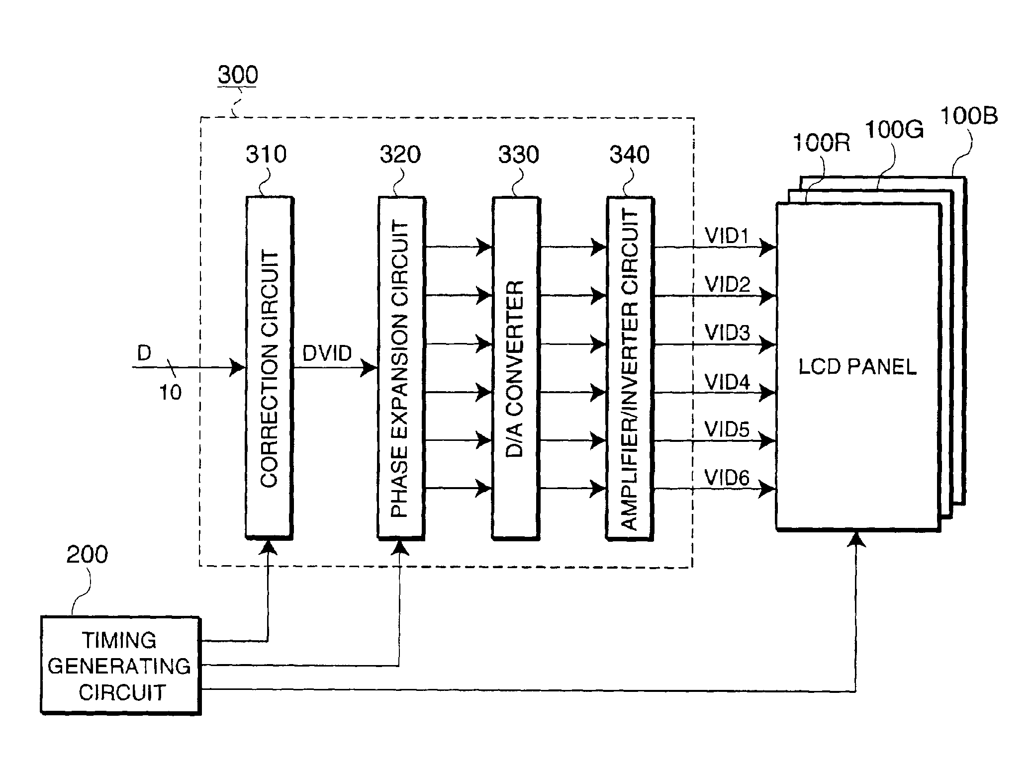
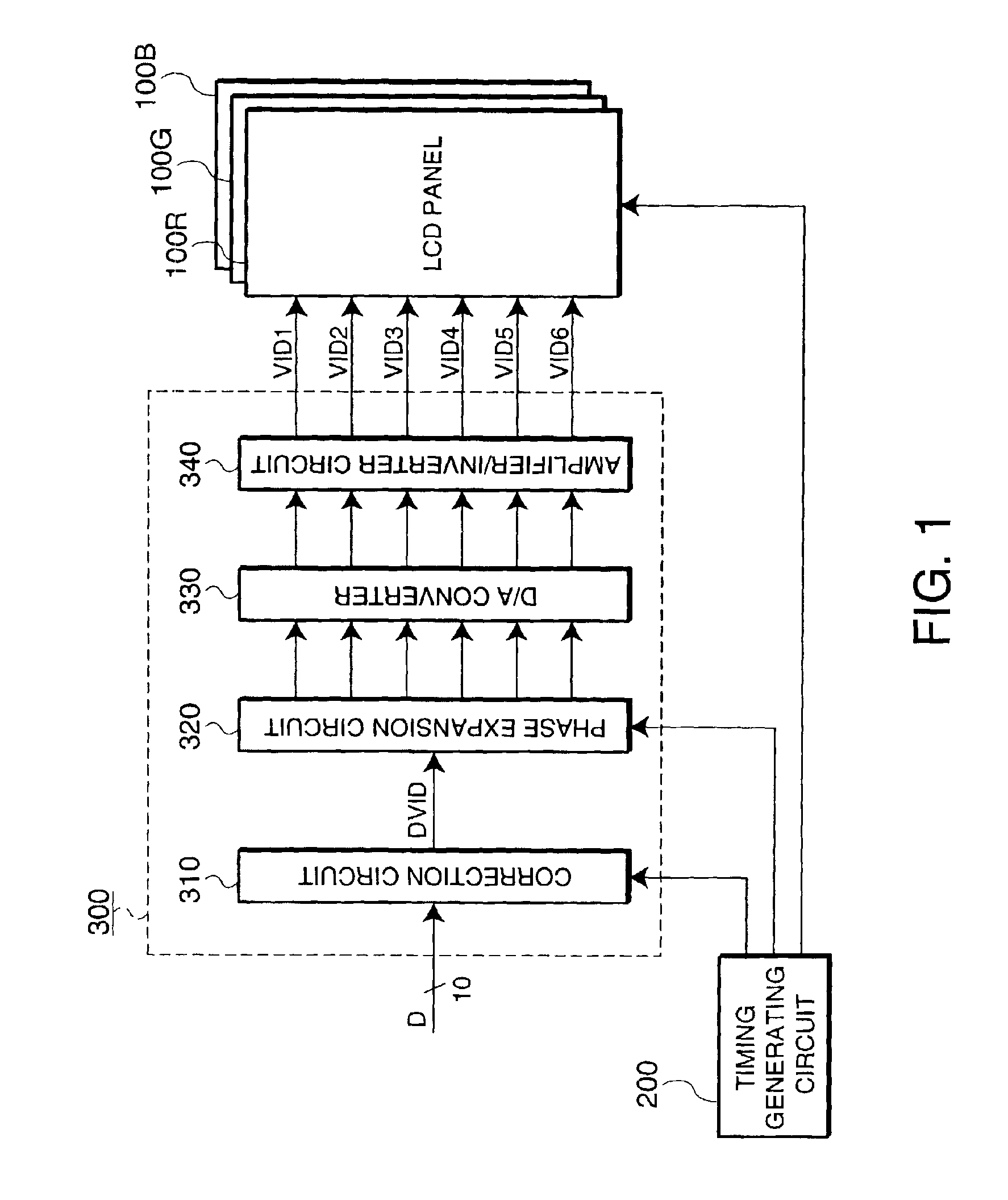
[0050]FIG. 1 is a schematic showing the electrical configuration of a projector. As shown in FIG. 1, a projector 1100 includes three LCD panels 100R, 100G, and 100B, a timing generating circuit 200, and an image processing circuit 300.
[0051]The LCD panels 100R, 100G, and 100B correspond to the three primary colors, namely, R (red), G (green), and B (blue). Each panel is formed by holding liquid crystal between a device substrate and an opposing substrate. In addition to a display region, a data-line driving circuit and a scanning-line driving circuit are formed in the periphery of the device substrate. In the following description, when a description is common to the three colors, the reference numeral “100” is collectively assigned to the LCD panels.
[0052]The timing generating circuit 200 supplies various timing signals to the scanning-line driving circuit, the data-line driving circuit, or the image processing circuit 300. The image processing circuit 300 generates phase-expanded ...
second embodiment
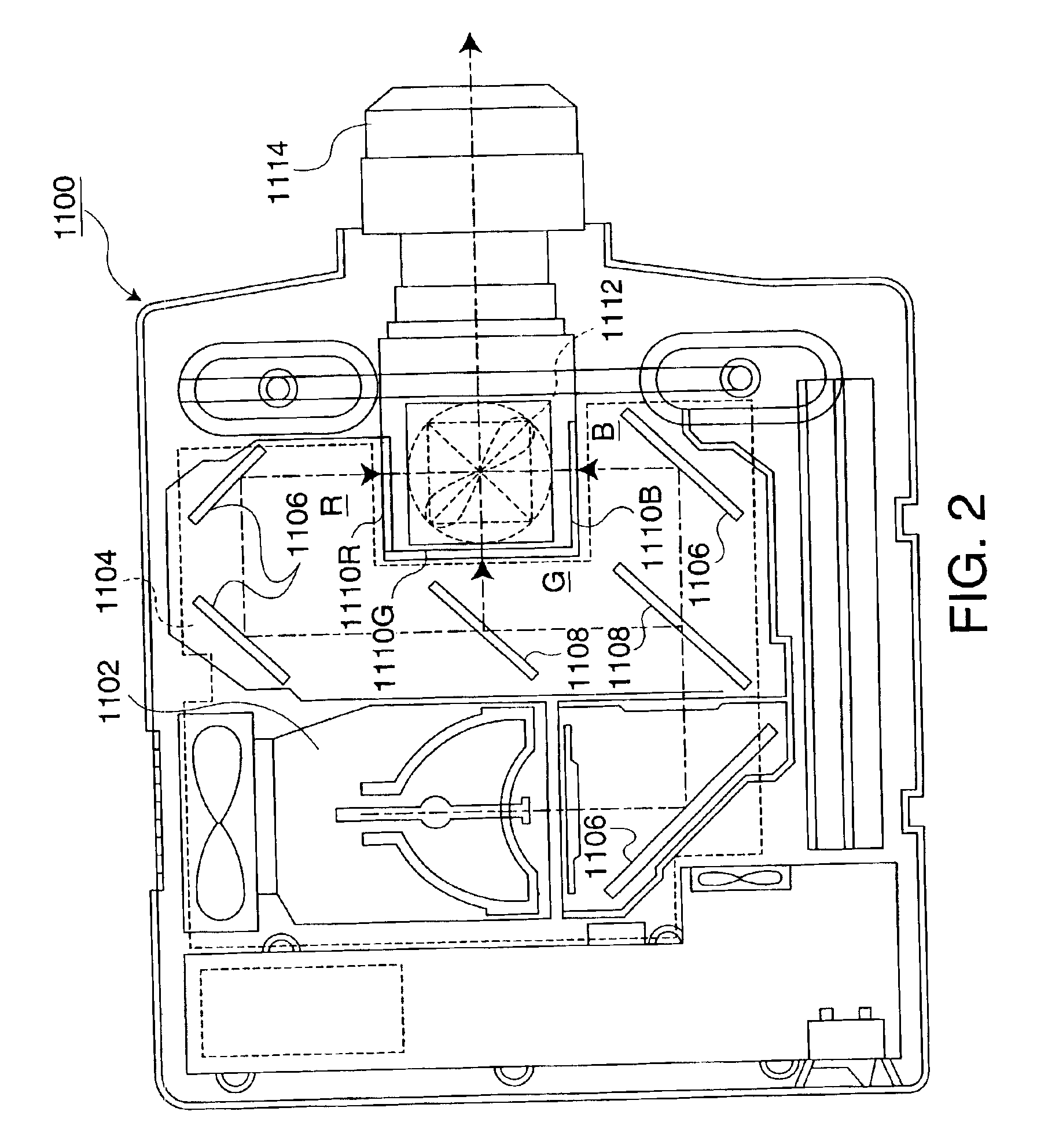
[0097]A projector according to a second embodiment will now be described. The electrical configuration of the projector of the second embodiment is similar to that of the projector of the first embodiment, which is shown in FIG. 1, except for the fact that an image processing circuit 300B is used in place of the image processing circuit 300A. The mechanical configuration of the projector of the second embodiment is similar to that of the projector of the first embodiment, which is shown in FIG. 2.
[0098]FIG. 11 is a schematic showing the electrical configuration of the projector according to the second embodiment. As shown in FIG. 11, the image processing circuit 300B of the second embodiment uses a D / A converter 330′ to convert the input image data Din into an analog signal. Subsequently, the analog signal is subjected to phase expansion, correction, and amplification / inversion. Thus, a phase expansion circuit 320′ differs from the phase expansion circuit 320, shown in FIG. 1, which...
PUM
| Property | Measurement | Unit |
|---|---|---|
| voltage | aaaaa | aaaaa |
| voltage | aaaaa | aaaaa |
| voltage | aaaaa | aaaaa |
Abstract
Description
Claims
Application Information
 - R&D
- Intellectual Property
- Life Sciences
- Materials
- Tech Scout
- Unparalleled Data Quality
- Higher Quality Content
- 60% Fewer Hallucinations
Browse by: Latest US Patents, China's latest patents, Technical Efficacy Thesaurus, Application Domain, Technology Topic, Popular Technical Reports.
© 2025 PatSnap. All rights reserved.Legal|Privacy policy|Modern Slavery Act Transparency Statement|Sitemap|About US| Contact US: help@patsnap.com