
Method and system for reducing leakage current in integrated circuits using adaptively adjusted source voltages

Active Publication Date: 2005-08-09
NAT SEMICON CORP
View PDF5 Cites 39 Cited by
  • Summary
  • Abstract
  • Description
  • Claims
  • Application Information

AI Technical Summary

Benefits of technology

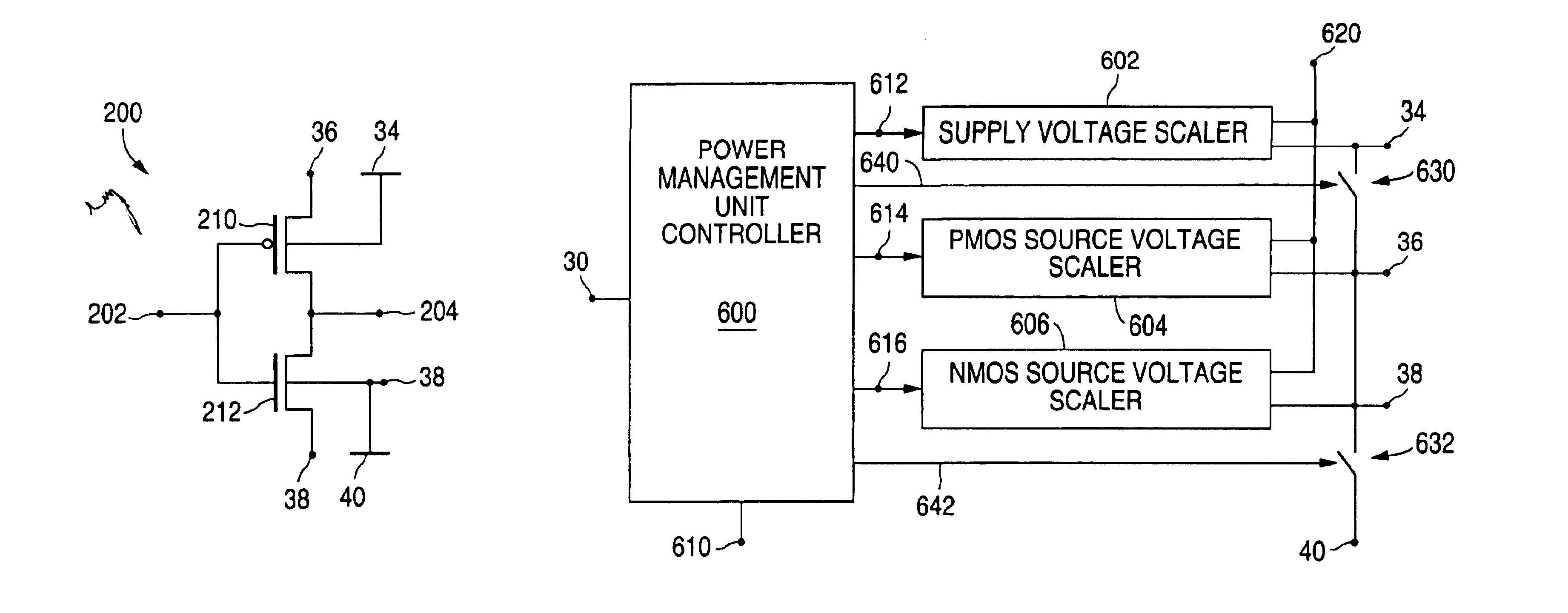
[0009]In accordance with the present invention, a method and system for reducing leakage current in integrated circuits using adaptively adjusted source voltages are provided that substantially eliminate or reduce disadvantages and problems associated with conventional systems and methods. According to an exemplary embodiment, the adaptively adjusted source voltages may be generated by, for example, a single inductor, multiple output (SIMO) switching regulator. In particular, adaptively adjusted source voltages are generated off-chip, while the bodies are held at the rails, making scaling for new technology easier and removing process-inherent sensitivities associated with on-chip methods.
[0010]To address the above-discussed deficiencies of the prior art, it is a primary object of the present invention to provide a method for reducing leakage current in integrated circuits using adaptively adjusted source voltages, the integrated circuits comprising PMOS and NMOS devices. According to an advantageous embodiment of the present invention, the method comprises: 1) applying a fixed VDD supply voltage to the bodies of the PMOS devices; 2) applying a fixed VSS supply voltage to the bodies of the NMOS devices; 3) applying an adjustable PMOS source voltage to sources of the PMOS devices; and 4) applying an adjustable NMOS source voltage to sources of the NMOS devices.
[0017]Technical advantages of one or more embodiments of the present invention include: 1) providing an improved method for reducing leakage current in integrated circuits, 2) allowing the use of higher efficiency switching regulators, and 3) requiring only one control loop. In a particular embodiment, adaptively adjusted source voltages are generated off-chip by decreasing a supply voltage and increasing a ground voltage, while the bodies are held at the rails. As a result, scaling for new technology is made easier. In addition, process-inherent sensitivities associated with on-chip methods are eliminated.

Problems solved by technology

However, voltage scaling does not provide much, if any, benefit for static power consumption due to leakage current.
This causes problems in digital technologies that have been scaled to be smaller and smaller, resulting in more leaky circuits.
In fact, the leakage current, which used to be a relatively small component of total power consumption, is actually dominating total power consumption for many deep submicron digital chips.
In typical mobile devices, this amount of leakage current, and its corresponding power consumption, is unacceptable.
However, threshold scaling does not provide much, if any, benefit for dynamic power consumption due to switching.
One drawback to this approach includes the use of a safety margin in the calculation of critical path delays when selecting the mode, which results in the chip possibly not operating at its optimum potential.
However, leakage current in the active or operating mode remains a problem with this approach and limits the battery life.
Both of these techniques are performed on-chip and suffer from process-inherent sensitivities, in addition to low quality analog process attributes of deep submicron processes such as leakage noise matching and the like.
Also, because this approach is on-chip, an inability to easily scale for new technology is another disadvantage.
Also, the use of a linear regulator does not allow total system power savings afforded by an external switching regulator.

Method used


Image

  • Method and system for reducing leakage current in integrated circuits using adaptively adjusted source voltages
  • Method and system for reducing leakage current in integrated circuits using adaptively adjusted source voltages
  • Method and system for reducing leakage current in integrated circuits using adaptively adjusted source voltages

Examples


Embodiment Construction

[0029]FIGS. 1 through 8, discussed below, and the various embodiments used to describe the principles of the present invention in this patent document are by way of illustration only and should not be construed in any way to limit the scope of the invention. Those skilled in the art will understand that the principles of the present invention may be implemented in any suitably arranged integrated circuit.

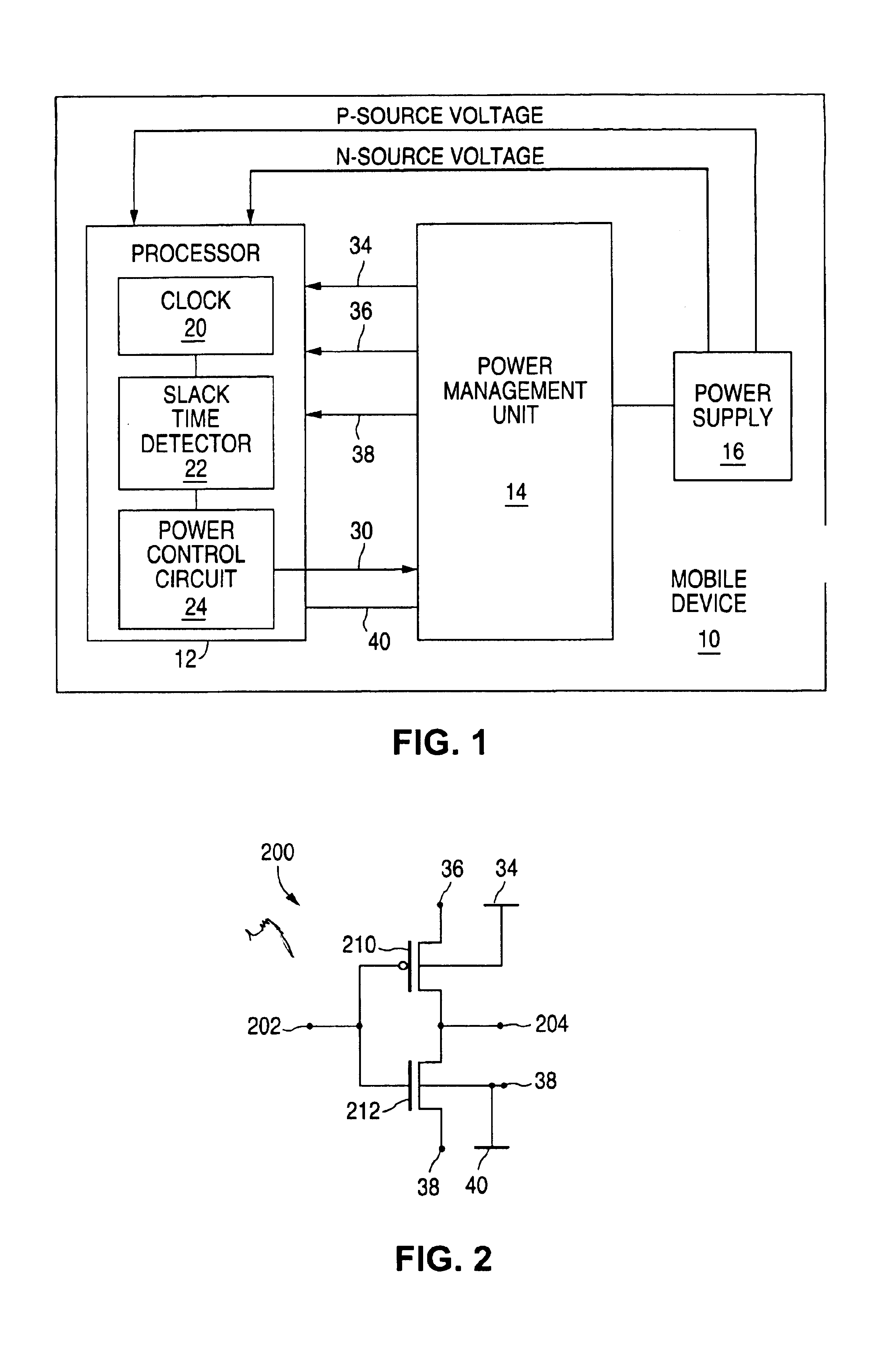
[0030]FIG. 1 is a block diagram illustrating a mobile device 10 that is operable to minimize power consumption using adaptively adjusted source voltages and using cooperative adaptive voltage and threshold scaling in accordance with one embodiment of the present invention. The mobile device 10 may comprise a mobile telephone, a personal digital assistant or any other suitable type of mobile device.

[0031]The mobile device 10 comprises a processor 12, a power management unit 14, and a power supply 16. The mobile device 10 also comprises other suitable components to enable its operatio...


PUM


Abstract

An apparatus for reducing leakage currents in an integrated circuit having logic gates containing PMOS devices and NMOS devices. The apparatus comprises a power management unit capable of: i) applying a fixed VDD supply voltage to body connections of said PMOS devices; ii) applying a fixed VSS supply voltage to body connections of said NMOS devices; iii) applying an adjustable PMOS source voltage to sources of said PMOS devices; and iv) applying an adjustable NMOS source voltage to sources of said NMOS devices.

Description

TECHNICAL FIELD OF THE INVENTION[0001]The present invention relates generally to power regulation for integrated circuits and, more particularly, to a method and system for reducing leakage current in integrated circuits using adaptively adjusted source voltages.BACKGROUND OF THE INVENTION[0002]Business and consumers use a wide array of wireless devices, including cell phones, wireless local area network (LAN) cards, global positioning system (GPS) devices, electronic organizers equipped with wireless modems, and the like. The increased demand for wireless communication, and other mobile devices has created a corresponding demand for technical improvements to such devices. Generally speaking, more and more of the components of conventional radio receivers and transmitters are being fabricated in a single integrated circuit package.[0003]One important aspect of wireless communication devices having integrated circuits is battery life. In order to maximize battery life for these wirel...

Claims


Application Information

Patent Timeline
IPC IPC(8): G05F1/10H03K19/00
CPCH03K19/0013
Inventor DOYLE, JAMES T.
Owner NAT SEMICON CORP
Learn More