Method for manufacturing a semiconductor device with a trench termination

Active Publication Date: 2005-07-26
INFINEON TECH AMERICAS
View PDF16 Cites 20 Cited by
  • Summary
  • Abstract
  • Description
  • Claims
  • Application Information

AI Technical Summary

Benefits of technology

[0002]The ever increasing demands for more efficient power supplies and longer lasting battery-powered electronic devices have made efficiency in power management systems one of the most challenging areas for engineers. Thus, improving the characteristics of discrete power devices, such as power MOSFETs, which are used in power management systems, continue to push manufacturers to produce devices with lower ON-resistance, lower gate charge and higher current capability.
[0003]A process according to the present invention significantly reduces the size of the features in a power device, resulting in reduced ON-resistance, reduced gate charge, and increased current carrying capability. As a result, a device, such as a power MOSFET, produced according to the present invention can be used in high frequency, e.g. 1 MHz, applications without undue heat generation. Thus, devices produced according to the present invention exhibit improved characteristics for power conversion.
[0005]The termination structure can significantly reduce the electrical field crowding at termination, thus eliminating the need for implanted guard rings without compromising the device breakdown voltage and ruggedness. Typical avalanche energy measured for this termination structure has been 1 J for a die in a DPAK.
[0006]The field oxide in the termination structure is grown using, for example, LOCOS process after the termination recess has been etched. Because the field oxide is below the top surface of the die, wafer planarity at active trench lithography stage is improved greatly. The much improved wafer surface planarity at trench lithography stage allows for further reduction of trench width by as much as 20%. This reduction in size makes it possible to, for example, increase the density of the trenches thus increasing channel density while keeping the gate charge low, especially the QGD and QSWITCH. To add to the performance of the device the depth of the channels may also be reduced.
[0007]A process according to the present invention includes forming source regions after high temperature steps have been carried out. As a result, the dimensions of the source regions can be minimized which allows for a reduction in the depth of the channel region and thus shorter channels in the device. The shorter channels in turn improve the ON-resistance of the device. In addition, shorter channels require a thinner epitaxial layer, as compared to prior art devices, thus reducing the cost of the device as well as further reducing the ON-resistance by shortening the common conduction region of the device.

Problems solved by technology

The ever increasing demands for more efficient power supplies and longer lasting battery-powered electronic devices have made efficiency in power management systems one of the most challenging areas for engineers.

Method used


Image

  • Method for manufacturing a semiconductor device with a trench termination
  • Method for manufacturing a semiconductor device with a trench termination
  • Method for manufacturing a semiconductor device with a trench termination

Examples


Embodiment Construction

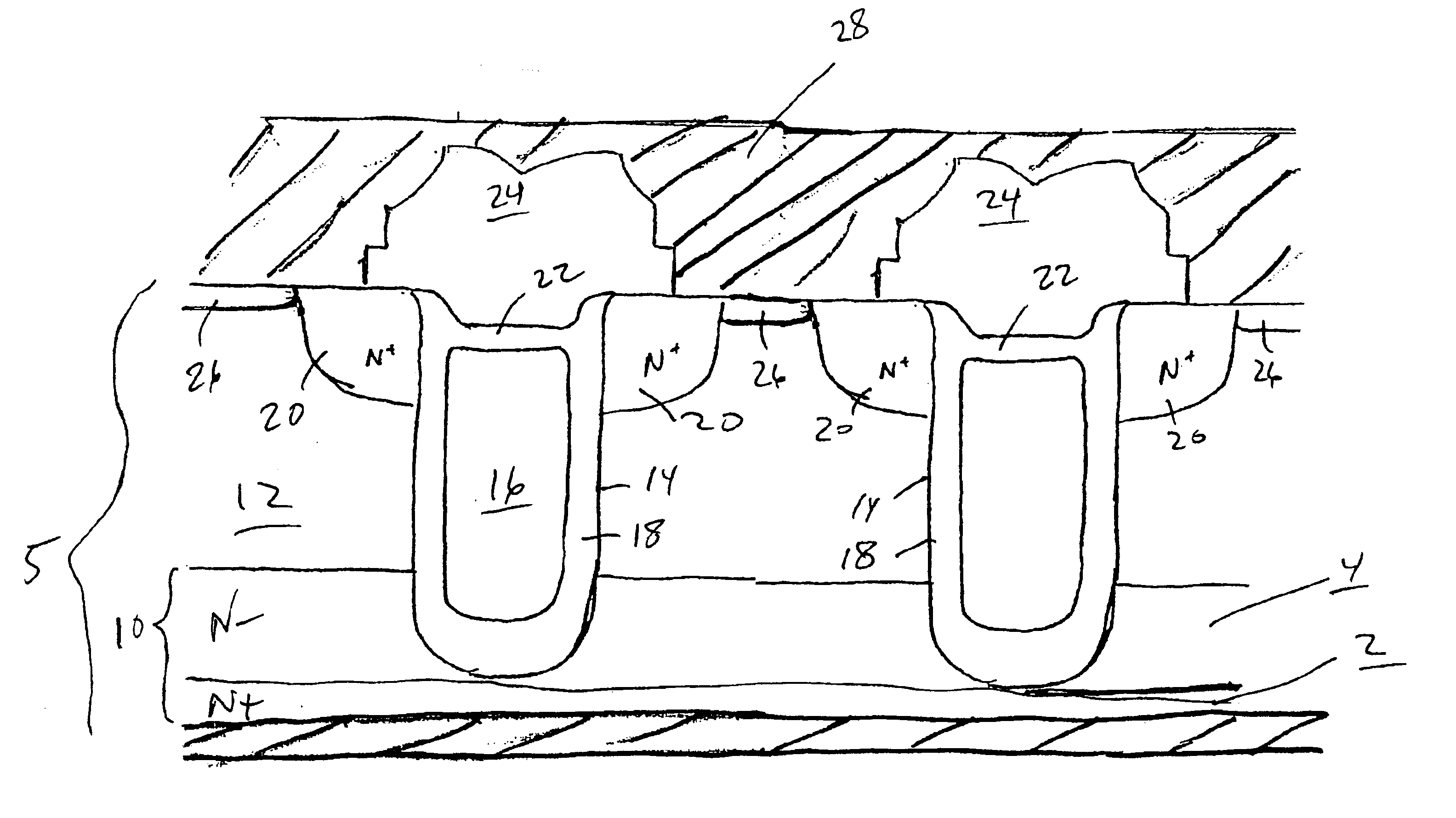
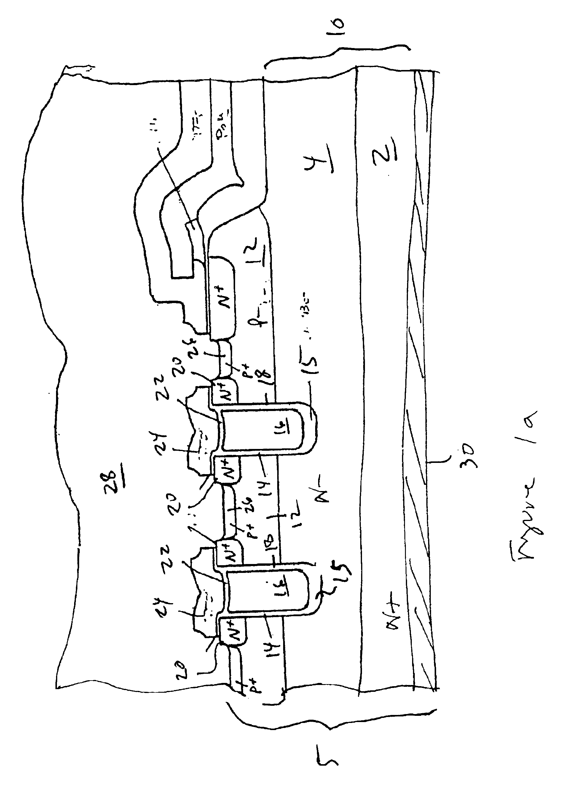
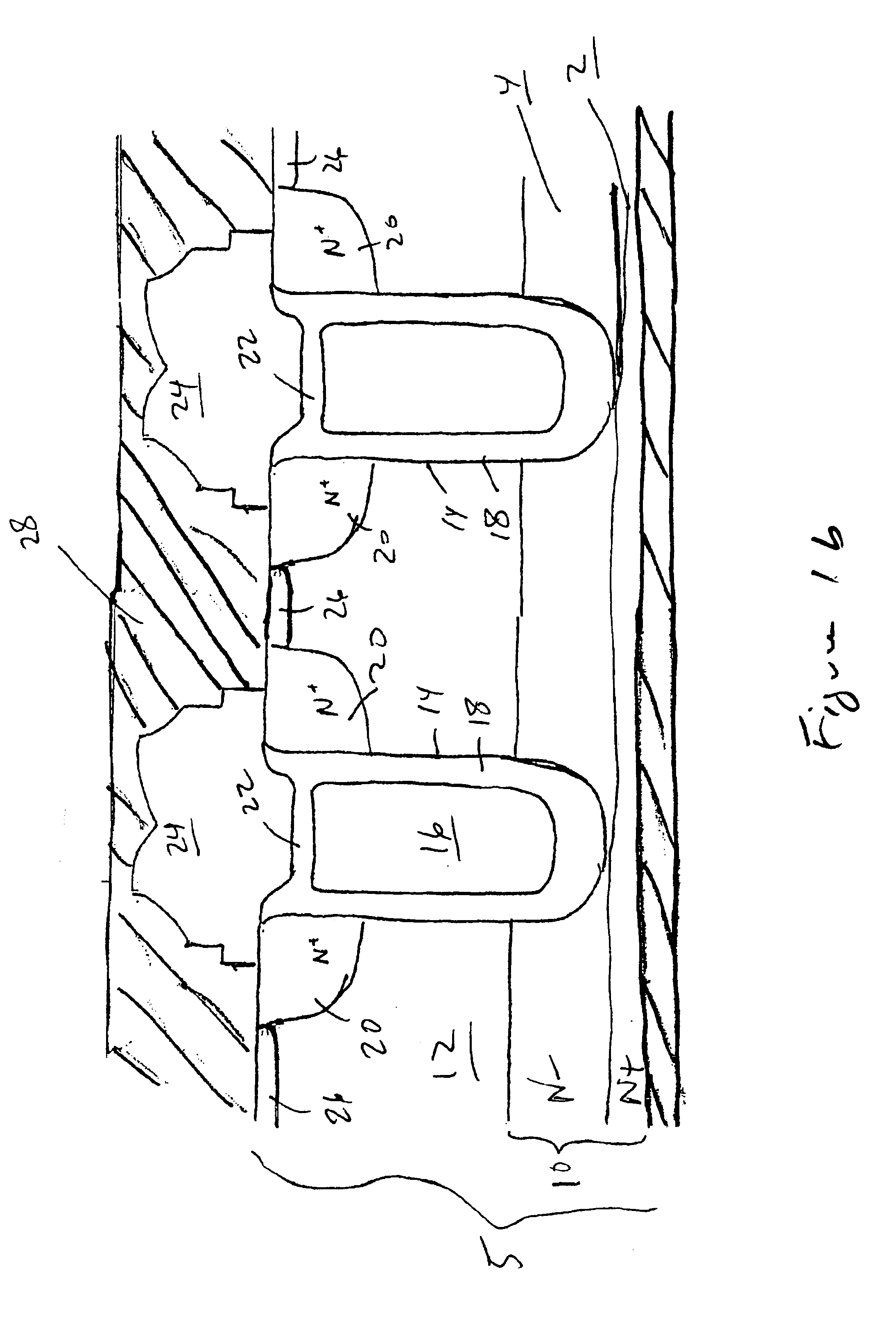
[0014]Referring to FIG. 1a, a semiconductor device according to the present invention is formed in silicon die 5 which includes drain region 10 of a first conductivity type, and channel region 12, which is lightly doped with dopants of a conductivity type that is opposite to those of drain region 10. A semiconductor device according to the present invention includes a plurality of trenches 14 extending from the top surface of die 5 to drain region 10. Trenches 14 have disposed therein conductive material such as doped polysilicon to form gate electrode 16. Gate electrodes 16 are electronically insulated from channel region 12 by oxide 18. Oxide 18 is formed at the side walls of each trench 14. It should be noted that a thick oxide 15 is formed at the bottom of each trench. A semiconductor device according to the present invention also includes self-aligned source regions 20 which are disposed on opposite sides of each trench 14 and extend to a predetermined depth less than the thick...


PUM


Abstract

A process for manufacturing a semiconductor device of the trench variety with reduced feature sizes and improved characteristics which process includes forming a termination structure having a field oxide disposed in a recess below the surface of the semiconductor die in which the active elements of the device are formed, and forming source regions after the major thermal steps have been performed.

Description

RELATED APPLICATIONS[0001]The application is based on and claims benefit of U.S. Provisional Application No. 60 / 415,302, filed on Sep. 30, 2002, entitled Self-Aligned Late Source with Photo Defined Contact Trench MOSFET, and U.S. Provisional Application No. 60 / 444,064, filed on Jan. 29, 2003, entitled Trench MOSFET Technology for DC—DC Converter Applications, to which claims of priority are hereby made.BACKGROUND AND SUMMARY OF THE INVENTION[0002]The ever increasing demands for more efficient power supplies and longer lasting battery-powered electronic devices have made efficiency in power management systems one of the most challenging areas for engineers. Thus, improving the characteristics of discrete power devices, such as power MOSFETs, which are used in power management systems, continue to push manufacturers to produce devices with lower ON-resistance, lower gate charge and higher current capability.[0003]A process according to the present invention significantly reduces the s...

Claims


Application Information

Patent Timeline
IPC IPC(8): H01L21/336H01L29/78H01L21/02H01L29/66H01L29/423H01L29/40H01L29/06
CPCH01L29/0661H01L29/407H01L29/66727H01L29/66734H01L29/7811H01L29/7813H01L29/42368
Inventor MA, LINGAMALI, ADAMKIYAWAT, SIDDHARTHMIRCHANDANI, ASHITAHE, DONALDTHAPAR, NARESHSODHI, RITUSPRING, KYLEKINZER, DANIEL
Owner INFINEON TECH AMERICAS
Why Eureka
Try Eureka