Semiconductor device and a method for checking state transition thereof

a semiconductor device and state transition technology, applied in the direction of electric controllers, pulse techniques, instruments, etc., can solve the problems of wasting a lot of time in evaluating entire combinations of commands at all timing, and it is difficult to generate trigger signals for this observation, so as to facilitate the evaluation and analysis of state transition, the effect of efficiently evaluating and analyzing state transitions

Active Publication Date: 2005-07-12
KIOXIA CORP
View PDF5 Cites 7 Cited by
  • Summary
  • Abstract
  • Description
  • Claims
  • Application Information

AI Technical Summary

Benefits of technology

[0018]The present invention intends to solve the above-mentioned problems. Accordingly, the present invention provides a semiconductor device and a checking method thereof for easily evaluating and analyzing the state transition by a state transition control mechanism. A sem

Problems solved by technology

Generally, it takes a very long time to write or erase the memory cells for a semiconductor device that installs asynchronous type memory cells, such as a nonvolatile memory.
This becomes a defect of a system installed in the semiconductor device since the writing operation takes a longer time than the operation time for another command cycle.
Meanwhile, it is a serious problem for evaluating such a condition of the semiconductor device to confirm all of the changes of the operations due to an interrupt command.
Particularly, this is a serious problem for such a semiconductor device that allows asynchronous input of an external signal, because it needs to take an extensive amount of time to perform an evaluation and a failure analysis.
In an evaluation method that inputs an interrupt command by simply shift

Method used


Image

  • Semiconductor device and a method for checking state transition thereof
  • Semiconductor device and a method for checking state transition thereof
  • Semiconductor device and a method for checking state transition thereof

Examples


first embodiment

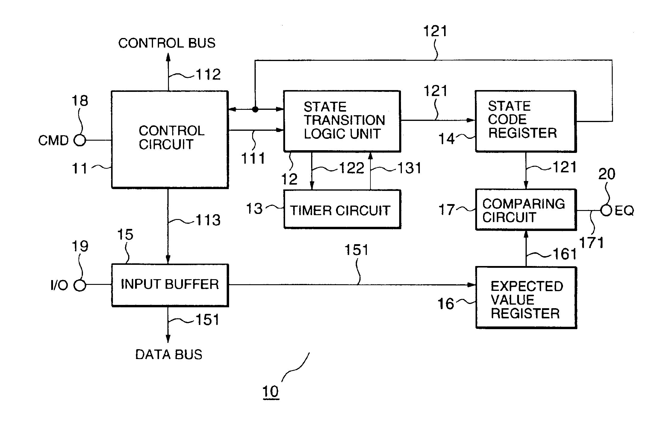
[0056]As illustrated in FIG. 3, the semiconductor device of this embodiment consistent with the present invention includes a control circuit 51 configured to generate a command or a control signal 211 by receiving an external signal through an input terminal 58, a state transition logic unit 52 configured to determine a next internal state based on a present internal state and the inputted command 211, a timer circuit 53 configured to count a residence period at the present internal state, a state code register 54 configured to hold a present internal state, an input buffer 55 configured to hold data inputted externally, an expected value register 56 configured to hold an internal state to be detected, and a comparing circuit 57 configured to compare between a present internal state 221 and an expected value 261 and to output an equal state signal 271. For simplifying the explanation, the necessary terms, such as internal state, state code, expected value, are defined as the same as...

second embodiment

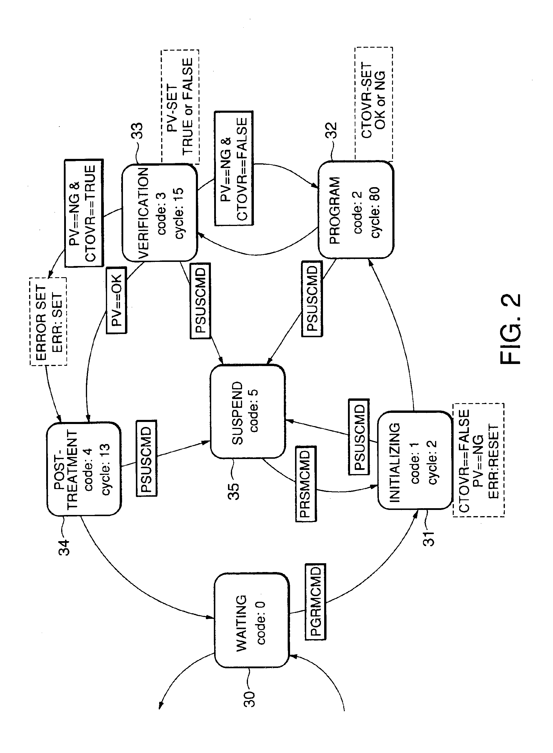
[0067]According to this second embodiment of the invention, it becomes possible to stop the state transition at a desired internal state by inputting an expected value corresponded to an arbitrary internal state. Thus, it can easily confirm a signal level at a desired internal state by a suitable method, such as an internal pin fitting. Especially, this embodiment is very useful for efficiently evaluating and analyzing a consecutive operation having a long execution time, such as a semiconductor device including nonvolatile memory cells. Consequently, this embodiment consistent with the present invention can largely improve efficiency for future development.

[0068]In this embodiment, it has been explained that the state transition from a stopped internal state as a result of a comparison to an expected value is executed by a PSUSCMD command. The present invention is not limited to this feature. For example, it is also possible to transit from each of the internal states to a waiting ...


PUM


Abstract

A semiconductor device includes a state code register that stores a state code representing a present internal state. A state transition logic unit is configured to determine a state code for a next internal state to be transited in accordance with a predetermined logic, based on a state code provided from the state code register and an input command instructing transition to a required state, and to set the determined state code into the state code register with synchronizing an internal clock. An expected value register is configured to hold an internal state to be detected, as an expected value code and a comparing unit compares the state code set in the state code register by the state transition logic unit to the expected value code in the expected value register and supplying an equal state signal when they coincide.

Description

BACKGROUND OF THE INVENTION[0001]1. Field of the Invention[0002]This application claims the benefit of priority from Japanese Patent Application No. 2003-19696, filed on Jan. 29, 2003 which, is hereby incorporated by reference in its entirety.[0003]The present invention relates to a semiconductor device that includes a state transition mechanism for controlling the transition of an internal state and to a method for checking a state transition thereof. More particularly, embodiments consistent with the present invention relate to a semiconductor device that includes a nonvolatile memory unit to perform an autonomic function for a partial state transition by using a timer circuit and to a method for improving evaluation efficiency of the semiconductor device.[0004]2. Description of Related Art[0005]Generally, it takes a very long time to write or erase the memory cells for a semiconductor device that installs asynchronous type memory cells, such as a nonvolatile memory. Further, duri...

Claims


Application Information

Patent Timeline
IPC IPC(8): G01R31/28G06F7/38G06F11/22G06F15/00G06F15/76G11C16/02G11C29/00H03K19/173G01R31/317G01R31/3177G01R31/3193G06F7/00G11C16/10G11C16/34G11C29/12
CPCG01R31/31703G01R31/3177G01R31/31932G11C16/10G11C16/3454G06F7/00
Inventor SAITO, HIDETOSHI
Owner KIOXIA CORP
Why Eureka
Try Eureka