
Magnetic logic element and magnetic logic element array

a logic element and array technology, applied in the field of magnetic logic element and magnetic logic element array, can solve the problems of large resistance, small career concentration of circuit elements, and increase in power consumption of integration, and achieve the effects of low power consumption of logic devices and/or memory devices, reduced size, and low resistan

Active Publication Date: 2005-07-05
KIOXIA CORP
View PDF5 Cites 53 Cited by
  • Summary
  • Abstract
  • Description
  • Claims
  • Application Information

AI Technical Summary

Benefits of technology

[0015]According to the embodiment of the invention, a magnetic logic element which has a logic processing function as well as a memory function with a reduced size, and the magnetic logic element array can be realized. As the result, small, high-density, and low power consuming logic devices and / or memory devices can be realized, and a merit on industry is great.

Problems solved by technology

However, these conventional elements functions only as a sensor or a memory.
However, these semiconductor circuit elements have small career concentration, and their resistance is essentially high.
Therefore, integration increases power consumption.
In addition, malfunction caused by downsizing also poses a problem.
Therefore, the further miniaturization is difficult.

Method used


Image

  • Magnetic logic element and magnetic logic element array
  • Magnetic logic element and magnetic logic element array
  • Magnetic logic element and magnetic logic element array

Examples


examples

[0197]Hereafter, the embodiments of the invention will be explained in more detail referring to the examples.

first example

[0198]First, as a first example of the invention, an element CL having a double tunnel junction which has the cross-sectional structure shown in FIG. 24 was fabricated. As shown in FIG. 24, the element CL has a semi hard layer HM1 made of Co—Fe alloy, a MR intermediate part MR1 made of Al2O3, a soft magnetic part SM made of Ni—Fe—Co alloy, a MR intermediate part MR2 made of Al2O3, and a semi hard layer HM2 made of Co—Fe alloy stacked in this order. These elements CL were arranged in the form of an array, as shown in FIG. 25. And the signal input was enabled by the magnetic field using the bit line BL and the word line WL.

[0199]In addition, in the element array shown in FIG. 25, one transistor (not shown) for cell selection was provided for every cell, and the word lines for selecting these transistors were also formed.

[0200]The magnetic body of the center of the element CL which has a double tunnel junction is soft magnetic part SM. Magnetization of this layer SM is changed accordin...

second example

[0204]Next, as a second example of the invention, the EOR memory which performs one EOR processing and records was produced by combining two elements of the first example mentioned above. Here, magnetization of the semi hard layers HM1 and HM2 was programmed rightward in FIGS. 22A and 22B. And after initializing magnetization of soft magnetic part SM rightward first, signal A and signal B were inputted into the first cell as they were, and both signals A and B were reversed and inputted into the second cell.

[0205]The truth tables obtained as the result were the same as Tables 1-4.

[0206]If a data signal is inputted as a signal A and an encryption key signal is inputted as a signal B, data can be saved as a stream cipher using two elements responding to one bit. Reproduction will be performed by reading the second cell, if the encryption key is “0”, and by reading the first cell, if the encryption key is “1”.


PUM


Abstract

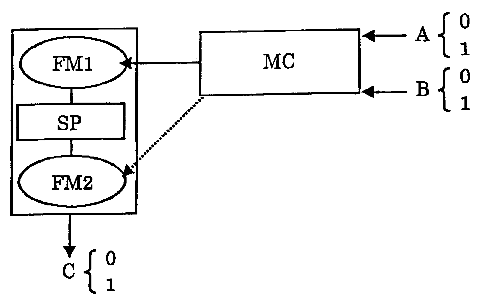
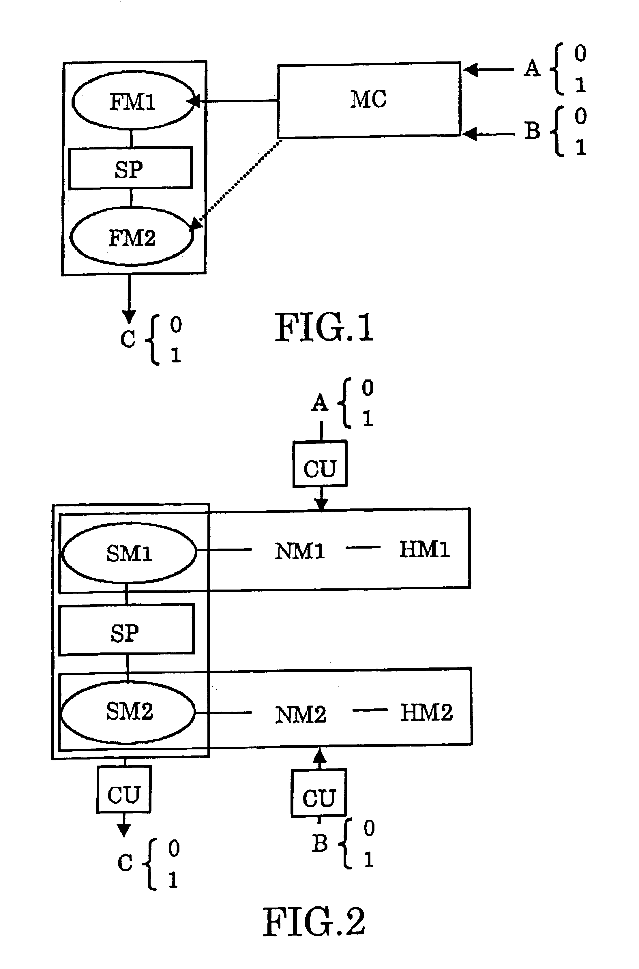
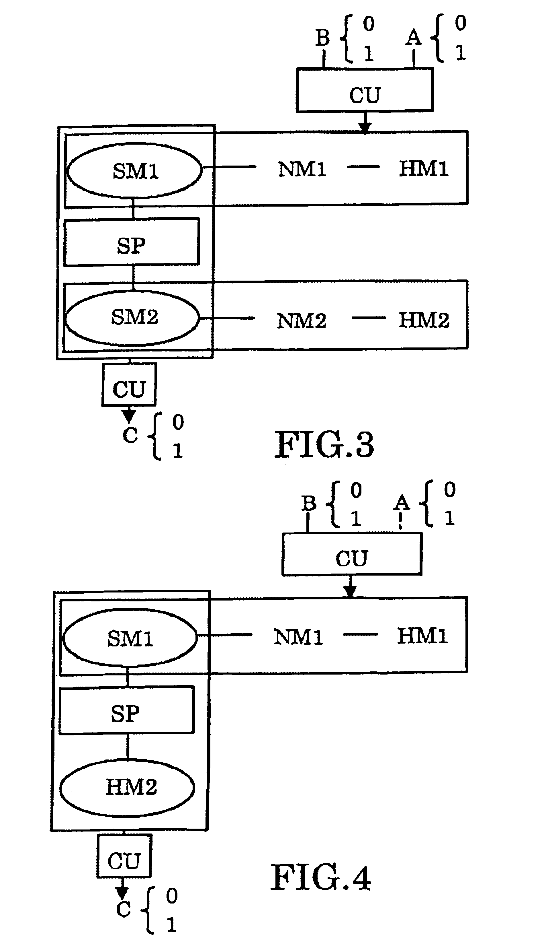
A magnetic logic element comprises a magnetic logic element cell having; a first and second magnetic parts; a MR intermediate part provided between the first and second magnetic parts. The magnetic logic element further includes a magnetization controlling part that controls a relation of directions of magnetizations of the first and second magnetic parts in accordance with a combination of a first binary input data and a second binary input data. A binary output data can be read by detecting a magnetoresistance effect of the first and second magnetic parts through the MR intermediate part.

Description

CROSS-REFERENCE TO RELATED APPLICATIONS[0001]This application is based upon and claims the benefit of priority from the prior Japanese Patent Application No. 2002-097445, filed on Mar. 29, 2002; the entire contents of which are incorporated herein by reference.BACKGROUND OF THE INVENTION[0002]This invention relates to a magnetic logic element and magnetic logic element array. More particularly, the invention relates to a magnetic logic element in which a recording of a direct-current-driving type and a reproduction by the magnetoresistance effect are possible, and a magnetic logic element array.[0003]Since the discovery that giant magnetoresistance effect (MR) is exhibited when a current is supplied to flow in parallel with the major plane of a multi-layered structure, efforts have been paid to find systems having still larger magnetoresistance ratios. Heretofore, ferromagnetic tunnel junction elements and CPP (current-perpendicular-to-plane) type MR elements in which electric curre...

Claims


Application Information

Patent Timeline
Patent Type & Authority Patents(United States)
IPC IPC(8): G11C11/16G11C11/02H03K19/02H03K19/168
CPCB82Y25/00G11C11/16H01F10/3263H03K19/168G11C11/161G11C11/1673G11C11/1675G11C11/15
Inventor NAKAMURA, SHIHOHANEDA, SHIGERU
Owner KIOXIA CORP
Learn More