Comparator with offset canceling function and D/A conversion apparatus with offset canceling function
a technology of offset canceling function and conversion apparatus, which is applied in the direction of pulse manipulation, pulse technique, instruments, etc., can solve the problems of difficult to provide a dedicated circuit and transmission error, and achieve the effect of high accuracy, simplified configuration and high accuracy
- Summary
- Abstract
- Description
- Claims
- Application Information
AI Technical Summary
Benefits of technology
Problems solved by technology
Method used
Image
Examples
embodiment 1
(Embodiment 1)
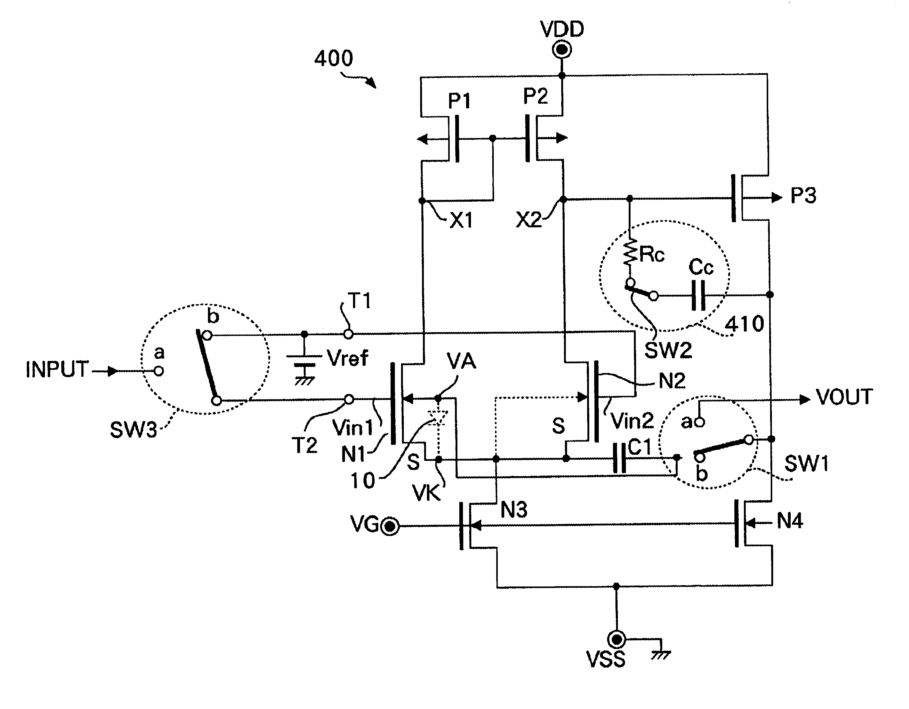
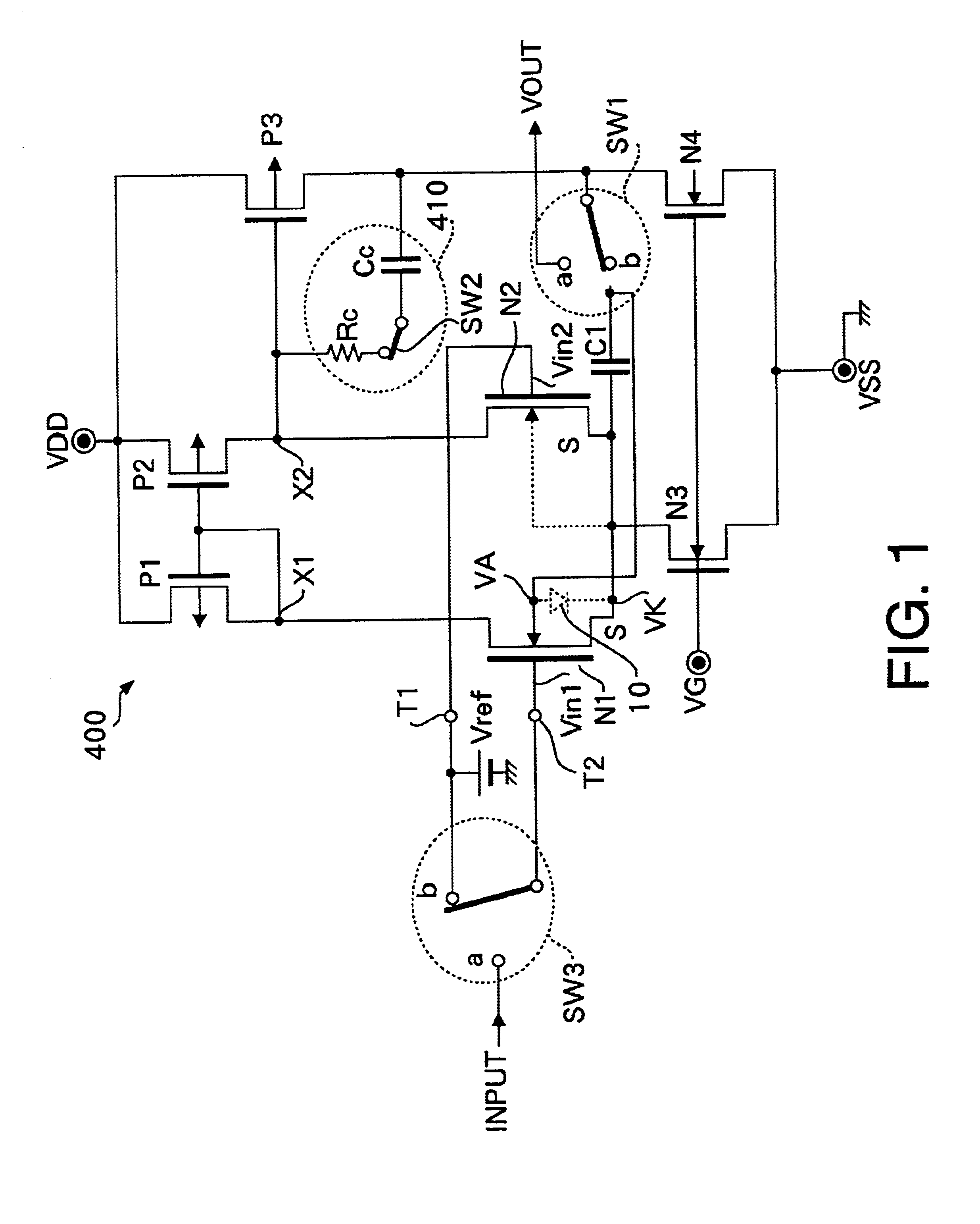
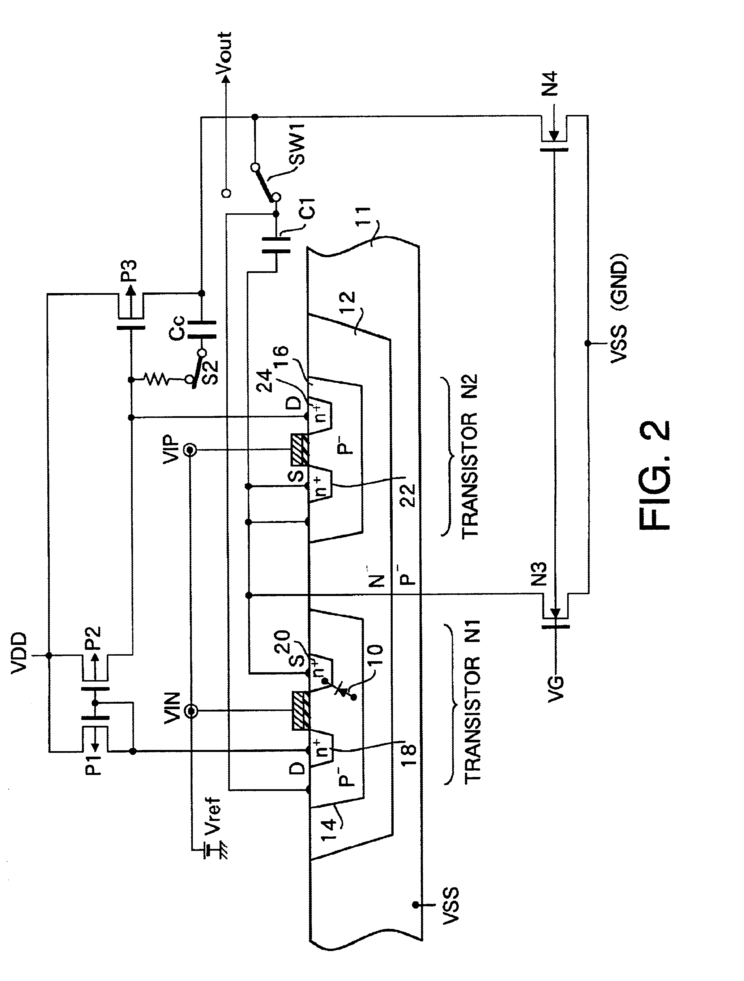
[0056]FIG. 1 is a circuit diagram showing a configuration example of a comparator with an offset canceling function of the present invention.
[0057]As illustrated, this comparator is constructed of NMOS transistors N1 and N2 forming a differential pair, constant current source transistor N3, load transistors (PMOS transistors) P1 and P2 forming a current mirror, output stage transistors (made up of PMOS transistor P3 and constant current source transistor N4) forming a push-pull type output stage circuit, phase adjustment circuit 410 (made up of phase adjustment resistor Rc, phase adjustment capacitance Cc and switch SW2 which turns ON during an offset adjustment), capacitor C1 and switches SW1 and SW3.
[0058]One differential pair transistor N1 is fed an input voltage (INPUT) or a reference voltage (also referred to as “bias voltage”: Vref) through input terminal T1.
[0059]The other differential pair transistor (N2) is always fed the reference voltage (Vref) through input...
embodiment 2
(Embodiment 2)
[0167]This embodiment cancels the input / output offset of the D / A converter included in the CDMA transmitter using the offset canceling function of the aforementioned embodiment.
[0168]FIG. 9A is a circuit diagram showing a circuit configuration for canceling an offset of a D / A converter. FIG. 9B is a block diagram showing a configuration of key components of a CDMA transmitter.
[0169]As shown in FIG. 9B, the CDMA transmitter converts two types of transmission data, I (in-phase) and Q (quadrature), output from spreader / modulator 300 to analog signals by D / A converters 500a and 500b respectively and transmits the signals from antenna 710 through QPSK modulator 600 and transmission circuit 700.
[0170]To prevent any phase error from occurring in the I and Q signals at this time, both D / A converters 500aand 500b must have identical input / output characteristics.
[0171]Thus, respective input / output offsets of D / A converters 500a and 500b are canceled using a negative feedback cir...
embodiment 3
(Embodiment 3)
[0185]FIG. 10 is a circuit diagram showing a configuration of a circuit to cancel offsets of a D / A converter of this embodiment.
[0186]The basic operation is the same as that in FIG. 9A. However, this embodiment uses addition / subtraction circuit 432 in correction value generation circuit 430. Switch SW4 is initially connected to the b terminal side.
[0187]Here, data equivalent to a 2 V DC voltage, which is the same as reference voltage Vref of comparator 400, is given as the input of adder 420. The initial value output from the addition / subtraction circuit is “0”.
[0188]Comparator 400 compares reference value Vref (=2V) and the input signal and if the input signal is larger, addition / subtraction circuit 432 subtracts a certain value (value equivalent to a predetermined step width).
[0189]On the contrary, if the input signal is smaller, addition / subtraction circuit 432 adds a certain value.
[0190]Thus, the loop goes on so as to make up for the offset in the input / output char...
PUM
 Abstract
Description
Claims
Application Information
 - R&D
- Intellectual Property
- Life Sciences
- Materials
- Tech Scout
- Unparalleled Data Quality
- Higher Quality Content
- 60% Fewer Hallucinations
Browse by: Latest US Patents, China's latest patents, Technical Efficacy Thesaurus, Application Domain, Technology Topic, Popular Technical Reports.
© 2025 PatSnap. All rights reserved.Legal|Privacy policy|Modern Slavery Act Transparency Statement|Sitemap|About US| Contact US: help@patsnap.com


