
IC card and manufacturing method thereof

a technology of ic card and manufacturing method, which is applied in the field of ic card, can solve the problems of weak conductive paste at mechanical deformation, difficult to manufacture contact pads and chip modules having the desired strength and durability, and achieve the effect of minimizing electric resistan

Inactive Publication Date: 2005-06-28
SAMSUNG TECHWIN CO LTD
View PDF7 Cites 31 Cited by
  • Summary
  • Abstract
  • Description
  • Claims
  • Application Information

AI Technical Summary

Benefits of technology

[0020]To solve the above and other problems, the present invention provides an IC card in which an electric resistance is minimized by directly connecting the antenna and the combi-chip.

Problems solved by technology

The conductive paste is a mixture of a plastic component exhibiting a high degree of hardness and conductive particles exhibiting no adhesiveness, and thus, the conductive paste is weak at mechanical deformation such as bending and cracks or a short circuit is easily generated.
Furthermore, since the chip module and the external contact pad are disposed in a card having a limited thickness, it is difficult to manufacture the contact pad and the chip module having a desired strength and durability.

Method used


Image

  • IC card and manufacturing method thereof
  • IC card and manufacturing method thereof
  • IC card and manufacturing method thereof

Examples


Embodiment Construction

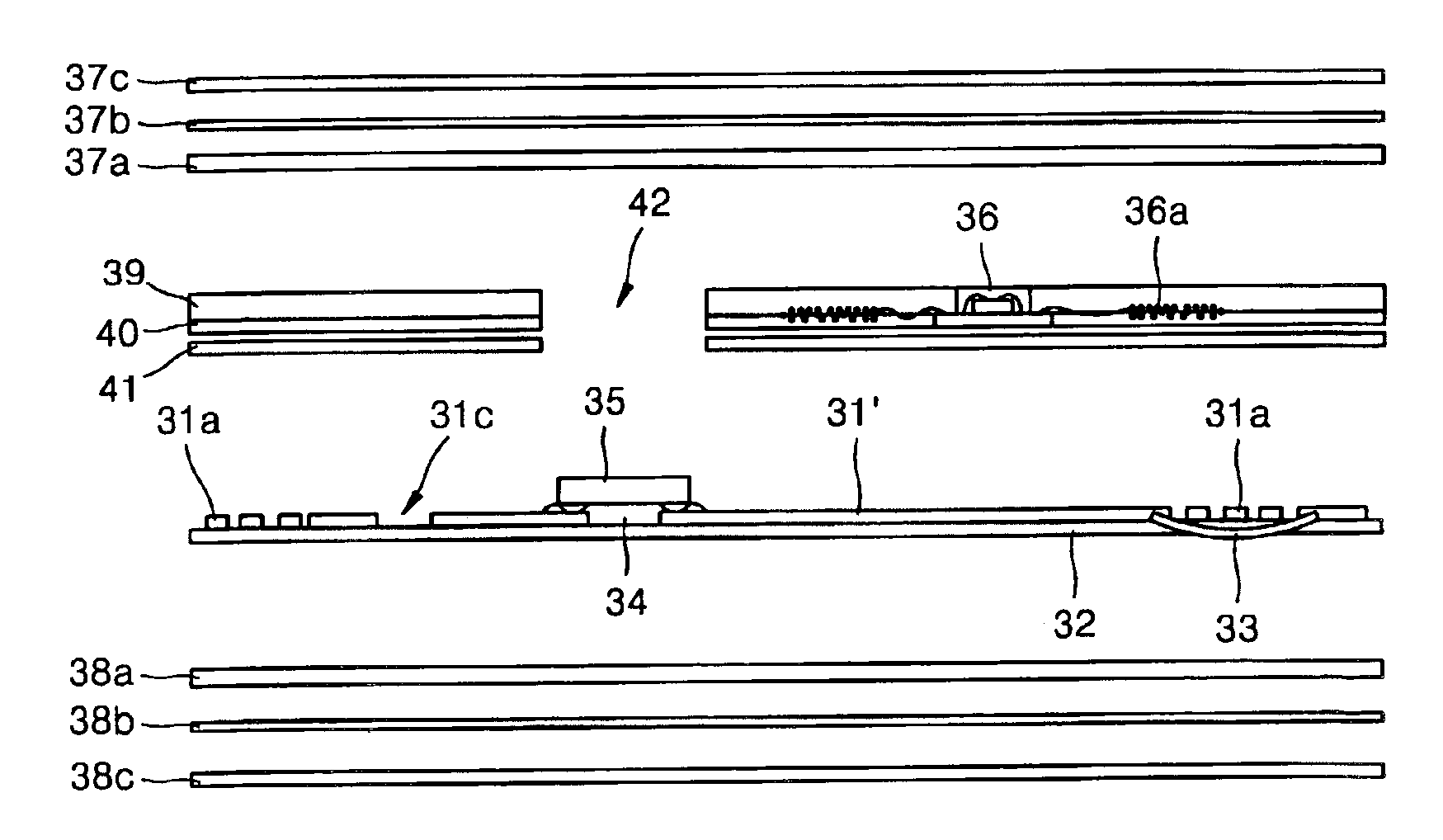
[0035]Referring to FIG. 3A, a clad layer 31 made of copper is formed on a film 32. The clad layer 31 is provided as a conductive layer to form a high frequency antenna pattern and a pattern for connection of a contact terminal (not shown).

[0036]Referring to FIG. 3B, the clad layer 31 is disposed on the film 32 to form a predetermined antenna circuit pattern 31′. The antenna circuit pattern 31′ can be formed in a typical method. For example, photoresist is coated on the clad layer 31 and then covered with a photomask. Thereafter, the photoresist is exposed and developed, and the clad layer 31 is etched. Then, an antenna pattern is formed by removing the photoresist. The antenna circuit pattern 31′ includes a wire shaped antenna portion 31a formed into a loop form, a connection portion 31b configured to mount a combi-chip having a chip bump (35a in FIG. 3F), and an attachment portion 31c to which an external contact pad 45 of FIG. 3K is mounted.

[0037]The wire-shaped antenna portion 31...


PUM


Abstract

An IC card includes an antenna circuit pattern formed on an insulation film and having a wire-shaped antenna portion, a portion corresponding to a chip bump of a combi-chip, and an attachment portion to which an external contact pad is attached. The combi-chip is attached to a portion corresponding to the chip bump of the combi-chip module on the antenna circuit pattern. At least one dielectric layer is attached to the antenna circuit pattern. An external contact pad is inserted in a hole formed in part of the dielectric layer and attached to the hole and has terminals formed in an outer surface and an inner surface of a substrate and connected to one another. The terminals on the inner surface contact the attachment portion is provided on the antenna circuit pattern.

Description

CROSS-REFERENCES TO RELATED APPLICATIONS[0001]This application claims priority from Korean Patent Application No. 2002-32517, filed on Jun. 11, 2002, in the Korean Intellectual Property Office, the disclosure of which is incorporated herein in its entirety by reference.BACKGROUND OF THE INVENTION[0002]1. Field of the Invention[0003]The present invention relates to an IC card and a method of manufacturing the same, and more particularly, to an IC card in which an antenna circuit pattern and a contact circuit board of a combi-chip provided in the IC card are directly connected so that an electric resistance therebetween is reduced, and a method of manufacturing the same.[0004]2. Description of the Related Art[0005]IC cards refer generally to cards on which IC chips are mounted and can be used as electronic identification (ID) cards, license cards, electronic money, and credit cards with various information stored in the IC chips. The term “IC card” used herein is intended to include “...

Claims


Application Information

Patent Timeline
IPC IPC(8): G06K19/077H05K3/28H05K1/11H05K1/14B42D15/10H01L25/00
CPCG06K19/07745G06K19/07749G06K19/07769G06K19/0775H01L2924/3025H01L2224/16227H01L2224/45139H01L2224/32225H01L2924/01087H01L2924/01068H05K3/284H05K1/141H05K1/11H01L2924/01079H01L2924/01078H01L2224/83192H01L2224/73204H01L2224/48227H01L2224/48091H01L2224/16225H01L2924/00014H01L2924/00H01L2924/00011H01L2924/01049H01L2224/45015H01L2924/207G06K17/00
Inventor KIM, DEOK-HEUNGKIM, CHANG-GYOOLEE, SEUNG-SEOB
Owner SAMSUNG TECHWIN CO LTD
Learn More