
Photo-patternable mono-phase fluorinated organometallic sol-gels for integrated optics and methods of fabrication

a mono-phase fluorinated, organometallic silane technology, applied in the field of photopatternable perfluorinated organometallic silane solgels, can solve the problems of increasing the scattering loss of the waveguide, complex and difficult implementation of ion implantation techniques, and not being compatible with standard silicon processing, etc., to achieve low bending loss and high refractive index

Inactive Publication Date: 2005-06-21
NP PHOTONICS A CORP OF DELAWARE
View PDF3 Cites 9 Cited by
  • Summary
  • Abstract
  • Description
  • Claims
  • Application Information

AI Technical Summary

Benefits of technology

[0024]In view of the above problems, the present invention provides a sol-gel material and methods of fabrication to produce high refractive index sol-gels directly fabricated onto silica-on-silicon substrates or photo-patterned into complex waveguide structures with low bending losses and propagation losses below 1 dB / cm at the telecommunication wavelengths.

Problems solved by technology

All of these techniques, in particular ion implantation, are complex and difficult to implement.
Ion exchange is performed on glass substrates and is not compatible with standard silicon processing.
These rough walls increase the scattering losses of the waveguide.
However, the fabrication of glasses generally requires high processing temperatures (T>1000° C.).
Such high temperatures are a severe limitation to the integration of waveguides into optoelectronic circuits.
Furthermore, sol-gel methods can produce compositions that are not possible with conventional methods.
Inorganic sol-gel films are usually limited to thin films because of the formation of cracks during polymerization and condensation in thick films (thickness>1 micrometer).
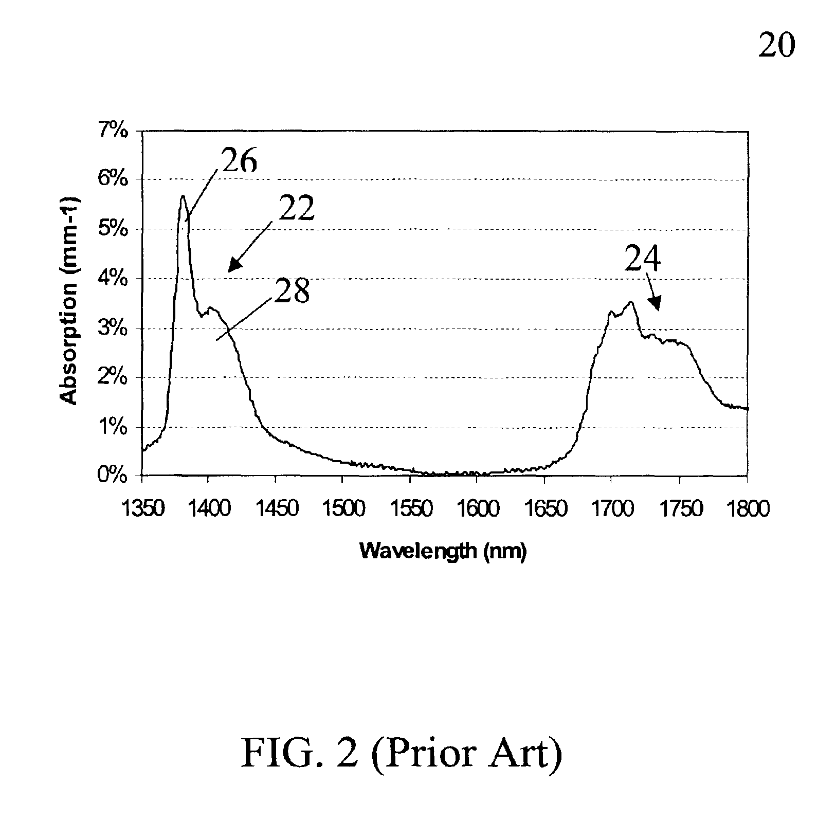
Unfortunately, conventional ORMOSILs have high optical loss at the telecommunication wavelengths due to a high concentration of carbon hydrogen and oxygen hydrogen bonds.
As mentioned above, this process often generates rough walls along the structures, which in turn generates optical scattering losses.
However, no methods to make low loss waveguides for the telecommunication wavelength are described.
However, the replacement of C—H bonds with C—F bonds is also known to reduce the refractive index of the material.
This is a problem because to define a waveguide in a sol-gel, the refractive index of the sol-gel must be higher than that of the substrate.
Following this approach, the index difference between cladding and the waveguide core is small and limits the optical confinement.
This in turn, limits the bending radii of the waveguide structures and consequently the footprint of complex waveguide structures such as arrayed waveguide gratings.
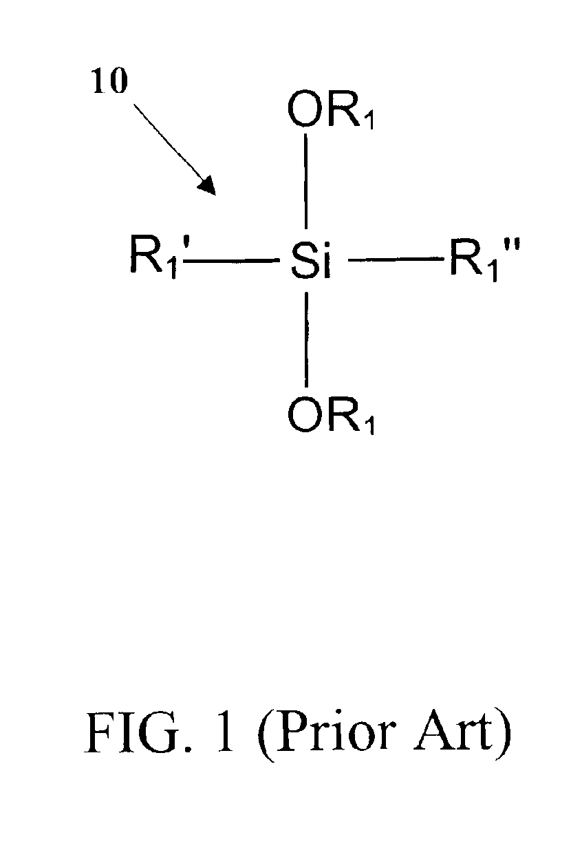
Unfortunately, organoalkoxysilane / metal oxide with general formula R1—[Si(O)3]n—[Ti(O)3]m—R1 are not photopatternable and have high optical loss.
Known sol-gels and methods of fabrication have failed to produce high refractive index sol-gels that can be directly fabricated onto silica-on-silicon substrates or photo-patterned into complex waveguide structures with low bending losses and propagation losses below 1 dB / cm at the telecommunication wavelengths.

Method used


Image

  • Photo-patternable mono-phase fluorinated organometallic sol-gels for integrated optics and methods of fabrication
  • Photo-patternable mono-phase fluorinated organometallic sol-gels for integrated optics and methods of fabrication
  • Photo-patternable mono-phase fluorinated organometallic sol-gels for integrated optics and methods of fabrication

Examples


example 1

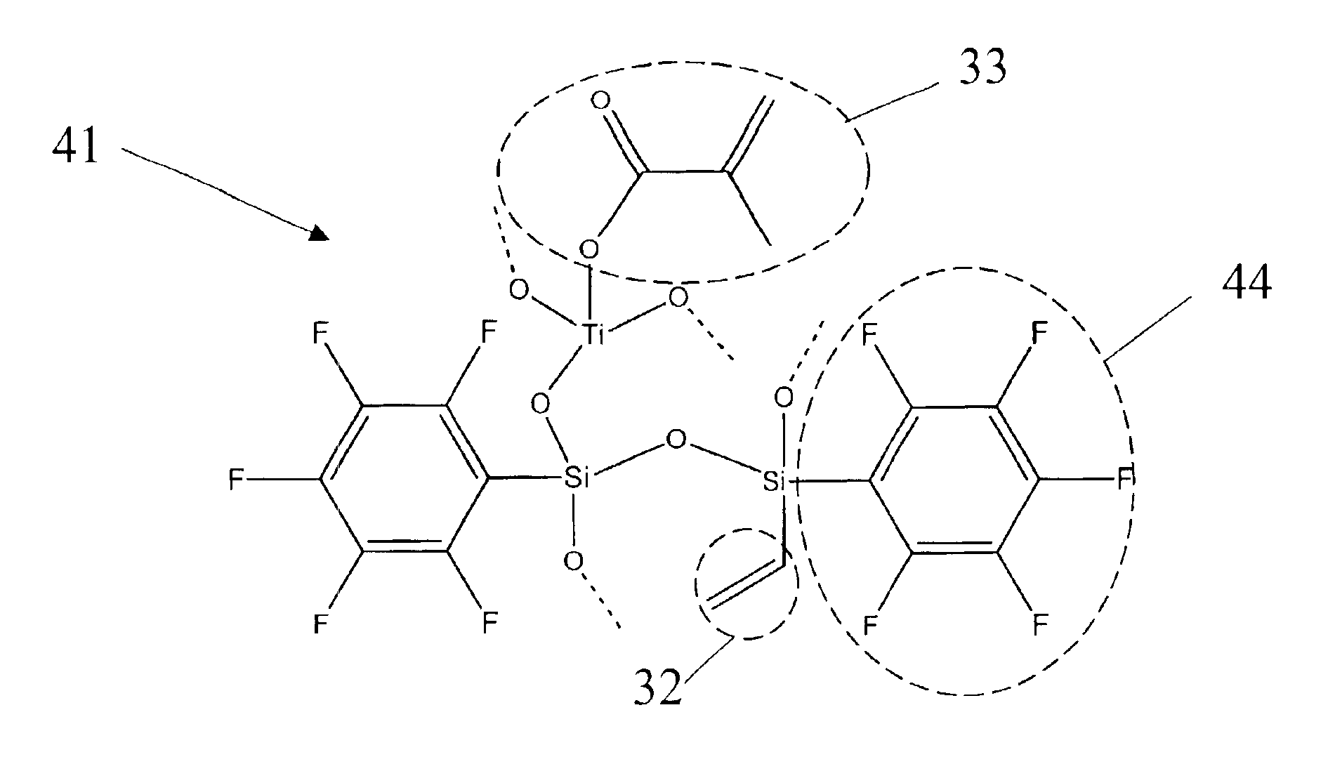
[0051]The sol-gel 41 described in FIG. 4a is prepared by mixing 2.31 ml of pentafluorophenyl triethoxy silane with 0.2 ml of aqueous (0.01 M) HCl and stirring for 30 minutes. 2.09 ml of pentafluorophenyl vinyl diethoxy silane is added and the solution is stirred for another 30 minutes. 0.16 ml of aqueous (0.01 M) HCl is added, stirred for 30 minutes, and 0.6 ml of tributoxytitanium methacrylate is added. The solution is stirred again for 30 minutes. 0.03 ml of H2O is added and the solution is stirred for 16 hours at ambient conditions. To obtain completely co-oligomer sol, all released solvents due to hydrolysis reaction are removed by rotavapor under reduced pressure 5 Torr for 60 min. After solvant removal, highly viscous co-oligomer sols with Ti surrounded by Si are obtained. The solution is aged for several hours, diluted with 5 ml of ethanol (Volume ratio of precursor and solvent is 1:1) and stirred for a few minutes, followed by adding 0.66 ml of H2O to complete hydrolysis. Af...

example 2

[0052]The preparation is carried out as in Example 1 except that pentafluorophenyl trimethoxy silane is used as a starting precursor. Since the molecular weight and density of each precursor is different, the relative volumes of precursors, aqueous HCl and water have to be adjusted for each composition to maintain the relative number of molecules per unit volume of all the constituents constant. In this example, 2.01 ml of pentafluorophenyl trimethoxy silane is mixed with 0.17 ml of aqueous (0.01 M) HCl and stirred for 30 minutes. 2.32 ml of pentafluorophenyl vinyl diethoxy silane is added and stirred for another 30 minutes. 0.17 ml of aqueous (0.01 M) HCl is added. After stirring the solution for 30 minutes, 0.67 ml of tributoxytitanium methacrylate is added. The solution is stirred again for 30 minutes. 0.04 ml of H2O is added and the solution is stirred for 16 hours at ambient conditions. To obtain completely co-oligomer sol, all released solvents due to hydrolysis reaction are r...

example 3

[0053]In this example, 2.6 ml of pentafluorophenyl triethoxy silane is mixed with 0.18 ml of aqueous (0.01 M) HCl and stired for 30 minutes. 1.72 ml of pentafluorophenyl vinyl dimethoxy silane is added and the solution is stirred for another 30 minutes. 0.18 ml of aqueous (0.01 M) HCl is added. After stirring the solution for 30 minutes, 0.68 ml of tributoxytitanium methacrylate is added. The solution is stirred again for 30 minutes. 0.04 ml of H2O is added and stirred for 16 hours at ambient conditions. To obtain completely co-oligomer sol, all released solvents due to hydrolysis reaction are removed by rotavapor under reduced pressure 5 Torr for 60 min. After removal of solvents, highly viscous co-oligomer sols with Ti surrounded by Si are obtained. The solution is then aged for several hours, diluted with 5 ml of ethanol (Volume ratio of precursor and solvent is 1:1) and stirred for a few minutes, followed by adding 0.78 ml of H2O to complete hydrolysis. After 30 minutes 0.03 ml ...


PUM

PropertyMeasurementUnit
Forceaaaaaaaaaa
Nanoscale particle sizeaaaaaaaaaa

Abstract

A photo-patternable perfluorinated silane sol-gel material is presented that exhibits a high refractive index and propagation losses below 1 dB / cm at the telecommunication wavelengths. The sol-gels are produced with general formula [(CH2)n,R′—Si(O)2]x—[Si(O)4]y—[R′—Si(O)3]z—[R″(CH2)n—M(O)3]w—[R′″(CH2)n—Si(O)3]v where O is oxygen, Si is silicon, M is a metal alkoxyde known to form bonds with organic compounds through oxygen donor ligands, and where , R″ and R′″ are photo cross-linkable groups, and where (CH2)n are alkyl spacers with n being an integer ≧0. The sol-gels can be fabricated to produce complex waveguide structures directly onto silica-on-silicon substrates with low bending losses.

Description

BACKGROUND OF THE INVENTION[0001]1. Field of the Invention[0002]This invention relates to photo-patternable perfluorinated organometallic silane sol-gels and methods to process the sol-gels into optical waveguides with low optical loss at the telecommunication wavelengths.[0003]2. Description of the Related Art[0004]With the rapid growth of integrated optics, passive and active waveguides are in high demand to implement routing, switching or filtering of optical information. Two-dimensional slab waveguides are obtained by depositing a thin film on a substrate, in which the film's refractive index is higher than that of the substrate and the medium above the film. Most waveguides for integrated optics also confine the optical radiation in the transverse direction leading to rectangular cross-sections with dimensions of a few micrometers. Such waveguides exist in various geometries, including the raised and embedded strip, rib or ridge, and strip-loaded waveguides. Dielectric waveguid...

Claims


Application Information

Patent Timeline
IPC IPC(8): G03F7/40G02B6/13G02B6/12G02B6/138G03F7/004G03F7/075G02B6/28
CPCG02B6/12004G02B6/138G03F7/0757G03F7/0043G02B2006/12097G02B6/2813
Inventor FARDAD, AMIRLIANG, WEIZHANG, YADONG
Owner NP PHOTONICS A CORP OF DELAWARE
Learn More