
Single transistor ferroelectric transistor structure with high-k insulator

a single-transistor, ferroelectric technology, applied in the direction of transistors, electrical devices, semiconductor devices, etc., can solve the problems of reducing the reliability of memory transistors, and achieve the effect of reducing or eliminating contamination

Inactive Publication Date: 2005-06-14
SHARP LAB OF AMERICA INC
View PDF13 Cites 30 Cited by
  • Summary
  • Abstract
  • Description
  • Claims
  • Application Information

AI Technical Summary

Benefits of technology

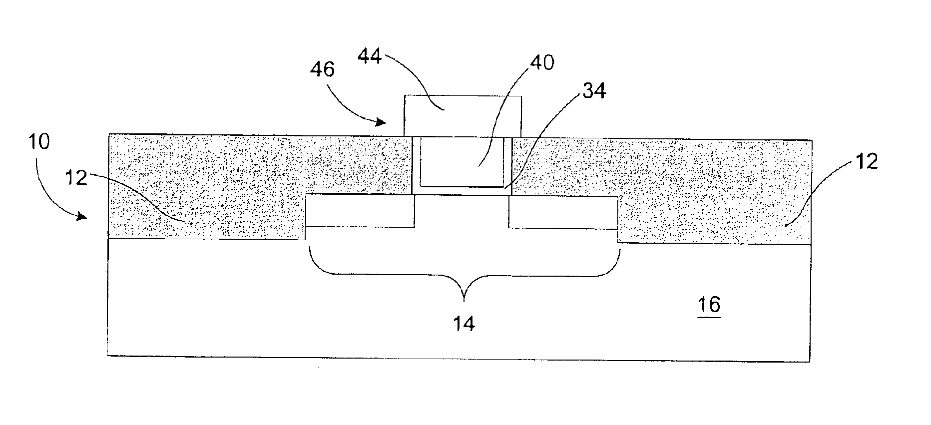
[0004]A ferroelectric transistor structure is provided comprising a ferroelectric gate overlying a semiconductor substrate. The ferroelectric gate has a bottom and sides surrounded by high-k material, and a top covered with a top electrode. The top electrode and the high-k material serve to encapsulate the ferroelectric gate, thereby reducing, or eliminating, contamination due to oxygen, hydrogen or other contaminants. The high-k material along the bottom of the ferroelectric gate also serves as a gate dielectric.

Problems solved by technology

Plasma etching degrades the ferroelectric properties of the ferroelectric gate, thereby reducing the reliability of the memory transistor.

Method used


Image

  • Single transistor ferroelectric transistor structure with high-k insulator
  • Single transistor ferroelectric transistor structure with high-k insulator
  • Single transistor ferroelectric transistor structure with high-k insulator

Examples


Embodiment Construction

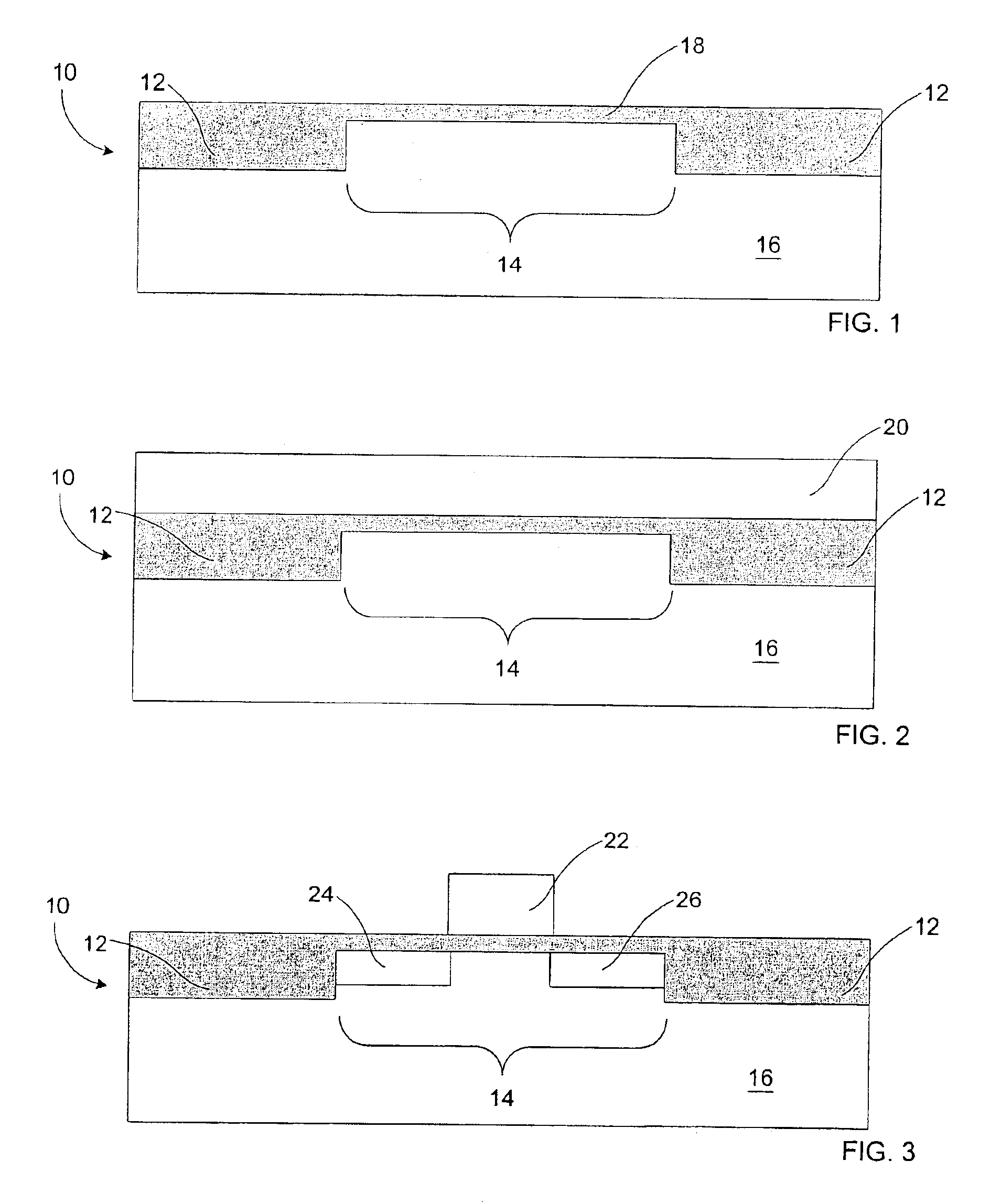
[0020]FIG. 1 shows a semiconductor structure 10 that has been prepared using state of the art processes. Shallow trench isolation (STI) has been used to produce isolation regions 12, and an active device region 14 on a substrate 16. Although an STI structure is shown, it would also be possible to use LOCOS isolation instead of STI. The semiconductor substrate is preferably silicon or silicon on insulator (SOI). A sacrificial oxide 18 has been grown or deposited over the substrate 16 to a thickness of between approximately 2 nm and 20 nm.

[0021]FIG. 2 shows a sacrificial layer 20 deposited overlying the sacrificial oxide 18. The sacrificial layer is deposited to a thickness of between approximately 200 nm and 400 nm. The sacrificial layer is preferably silicon nitride or polysilicon. The sacrificial layer is preferably easy to remove by selective etching without affecting underlying or adjacent materials.

[0022]FIG. 3 shows a sacrificial gate structure 22 formed by patterning the sacri...


PUM


Abstract

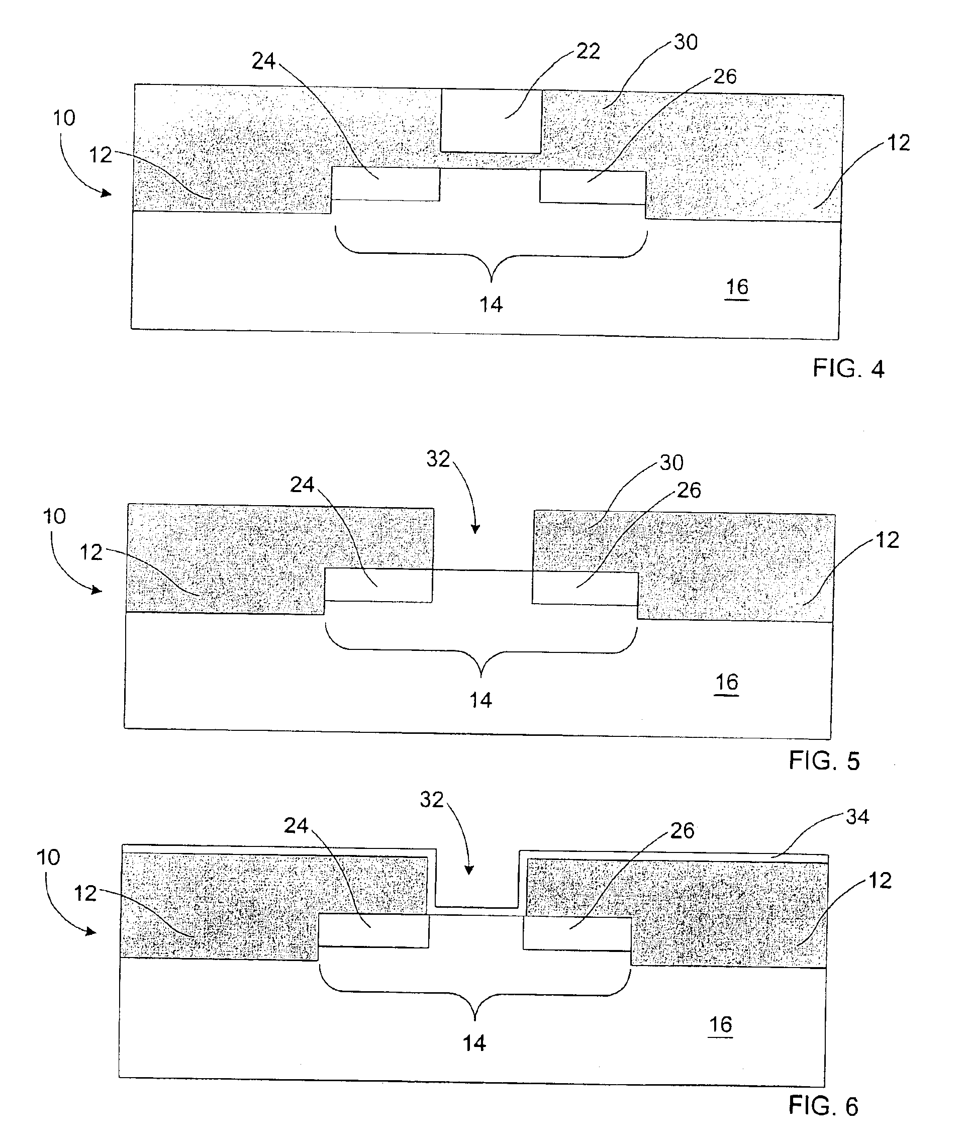
A ferroelectric transistor gate structure with a ferroelectric gate and a high-k insulator is provided. The high-k insulator may serve as both a gate dielectric and an insulator to reduce, or eliminate, the diffusion of oxygen or hydrogen into the ferroelectric gate. A method of forming the ferroelectric gate structure is also provided. The method comprises the steps of forming a sacrificial gate structure, removing the sacrificial gate structure, depositing a high-k insulator, depositing a ferroelectric material, polishing the ferroelectric material using CMP, and forming a top electrode overlying the ferroelectric material.

Description

CROSS-REFERENCE[0001]This application is a divisional of application Ser. No. 09 / 820,023, filed Mar. 28, 2001, entitled “Single Transistor Ferroelectric Transistor Structure with High-k Insulator and Method of Fabricating Same,” invented by Sheng Teng Hsu, and Fengyan Zhang, now U.S. Letters Patent No. 6,602,720, which is hereby incorporated by reference.BACKGROUND OF THE INVENTION[0002]This invention relates generally to semiconductor technology and more particularly to metal-ferroelectric-insulator semiconductor (MFIS) transistor structures, and methods of fabrication. An MFIS transistor is similar to an MFOS transistor, but is not limited to structures that use oxide as the insulator material.[0003]Previously, single transistor ferroelectric memory transistors have utilized a ferroelectric electrode stack, comprising a ferroelectric gate with a top electrode. The device would be formed by depositing a ferroelectric material, followed by an overlying metal layer. The layers would ...

Claims


Application Information

Patent Timeline
Patent Type & Authority Patents(United States)
IPC IPC(8): H01L21/336H01L21/02H01L29/78H01L21/28H01L29/51H01L29/66H01L29/49H01L29/40H01L21/3105H01L21/316H01L21/8246H01L27/105H01L21/8247H01L29/788H01L29/792
CPCH01L21/02189H01L21/02197H01L21/02271H01L21/0228H01L21/28291H01L29/78391H01L29/4983H01L29/516H01L29/66545H01L21/31604H01L21/31691H01L21/31053H01L29/40111H01L21/18
Inventor HSU, SHENG TENGZHANG, FENGYAN
Owner SHARP LAB OF AMERICA INC
Learn More