Vacuum packaged micromirror arrays and methods of manufacturing the same
a technology of vacuum packaging and micromirror arrays, applied in the field of vacuum packaging micromirror arrays, to achieve the effects of improving manufacturing yield, improving dielectric isolation, and improving optical isolation of the control circuit area
- Summary
- Abstract
- Description
- Claims
- Application Information
AI Technical Summary
Benefits of technology
Problems solved by technology
Method used
Image
Examples
Embodiment Construction
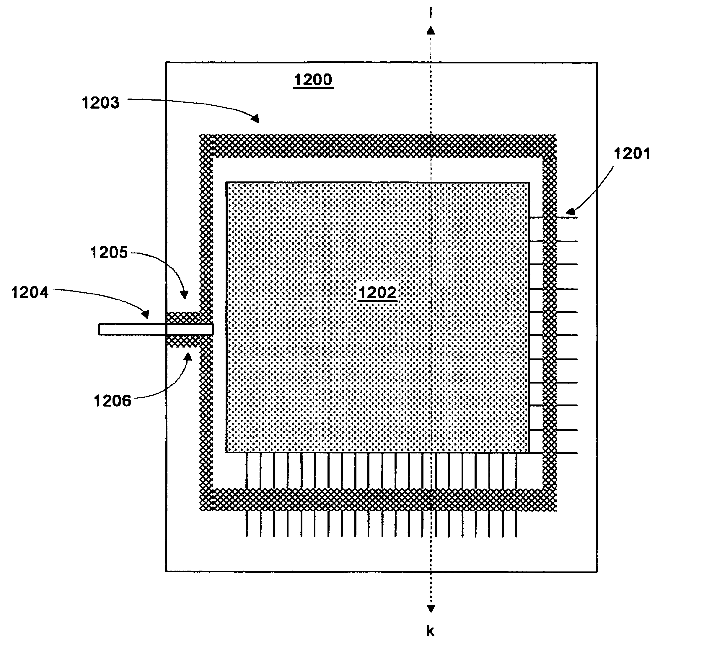
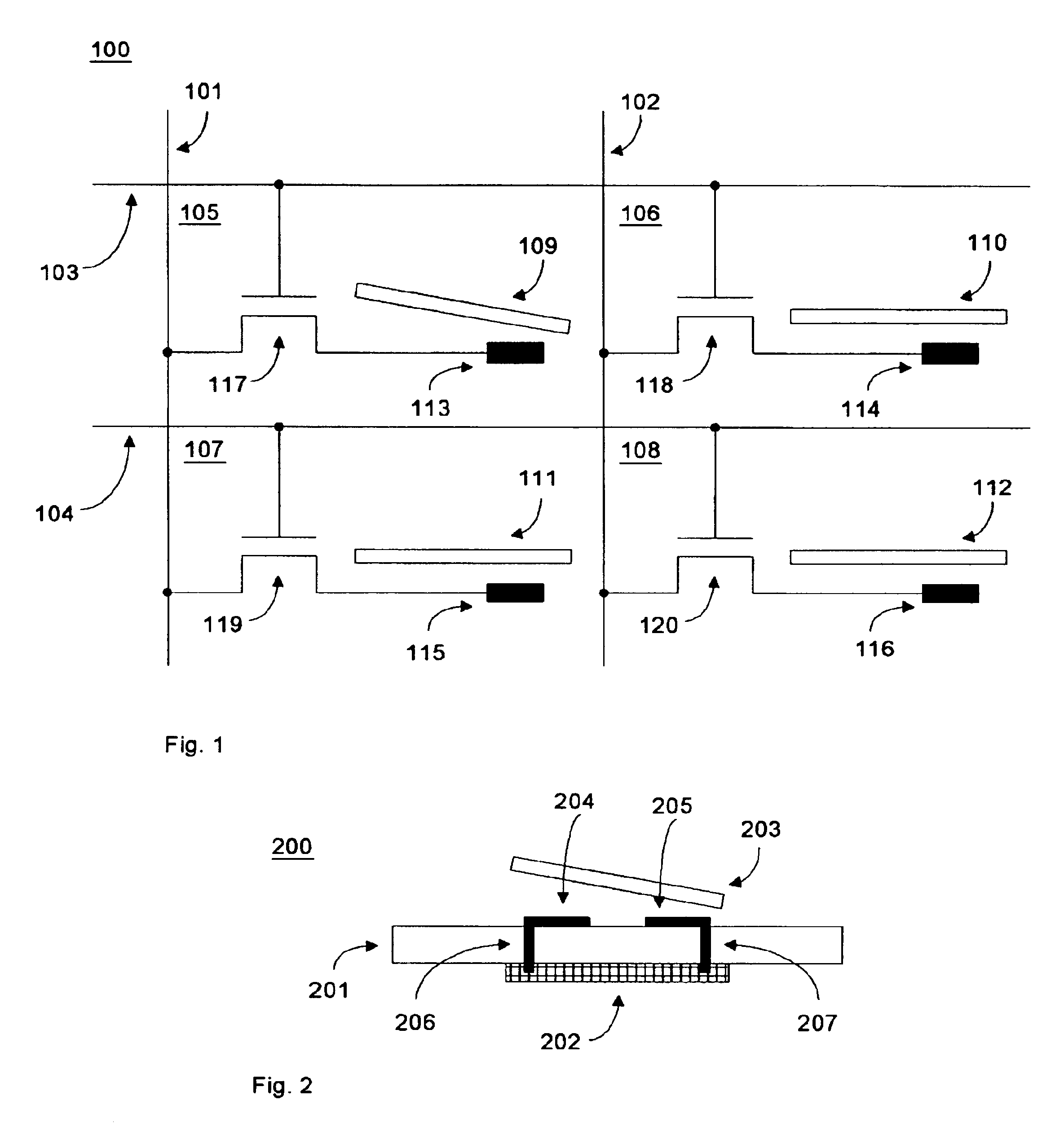
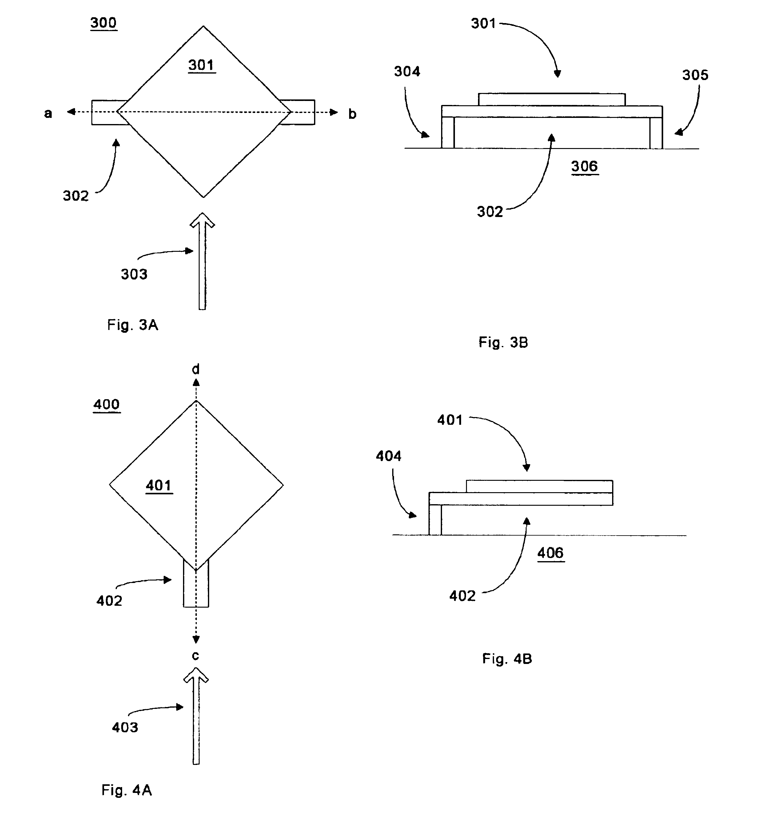
[0055]The present invention relates to electromechanical micromirror devices and arrays of such devices. Shown schematically in FIG. 1 is an array 100 comprising vertical data lines (101 and 102) and horizontal addressing lines (103 and 104), with each intersection of these data and addressing lines forming an electromechanical micromirror device (105, 106, 107, and 108). Each micromirror device comprises a micromirror (109, 110, 111, and 112), an addressing electrode (113, 114, 115, and 116), and an NMOS transistor (117, 118, 119, and 120). Micromirror 109 is shown to be in a deflected state while the other micromirrors are in their undeflected states. A possible scheme for addressing the micromirrors is as follows: The micromirrors (109, 110, 111, and 112) are electrically connected to ground. The deflection of a micromirror is determined by the bias voltage between the micromirror and its addressing electrode. The desired bias voltage is set by the voltages on the vertical data l...
PUM
 Abstract
Description
Claims
Application Information
 - R&D
- Intellectual Property
- Life Sciences
- Materials
- Tech Scout
- Unparalleled Data Quality
- Higher Quality Content
- 60% Fewer Hallucinations
Browse by: Latest US Patents, China's latest patents, Technical Efficacy Thesaurus, Application Domain, Technology Topic, Popular Technical Reports.
© 2025 PatSnap. All rights reserved.Legal|Privacy policy|Modern Slavery Act Transparency Statement|Sitemap|About US| Contact US: help@patsnap.com


