
Gain amplifier with DC offset cancellation circuit

a technology of offset cancellation and gain amplifier, which is applied in the direction of pulse manipulation, pulse technique, instruments, etc., can solve the problems of unavoidable dc offset and observe dc offset, and achieve the effect of reducing convergence tim

Active Publication Date: 2005-06-07
IND TECH RES INST
View PDF4 Cites 31 Cited by
  • Summary
  • Abstract
  • Description
  • Claims
  • Application Information

AI Technical Summary

Benefits of technology

[0003]The main objective of the present invention is to provide a gain amplifier with a DC offset cancellation circuit. By applying multiple sets of feedback factors for reducing convergence time, the DC offset of the signals can be cancelled.

Problems solved by technology

As a result of coupling of the RF input to local oscillators, due to input of mixers in the applied architectures for low intermediate frequency (low IF) and zero intermediate frequency (zero IF), it is highly likely that interference resulting from signals being mixed will be introduced, resulting in unavoidable DC offset.
Furthermore, due to mismatch of components or manufacturing process flaws, the DC offset can also be observed in integrated circuits used in gain amplifier circuits.

Method used


Image

  • Gain amplifier with DC offset cancellation circuit
  • Gain amplifier with DC offset cancellation circuit
  • Gain amplifier with DC offset cancellation circuit

Examples


Embodiment Construction

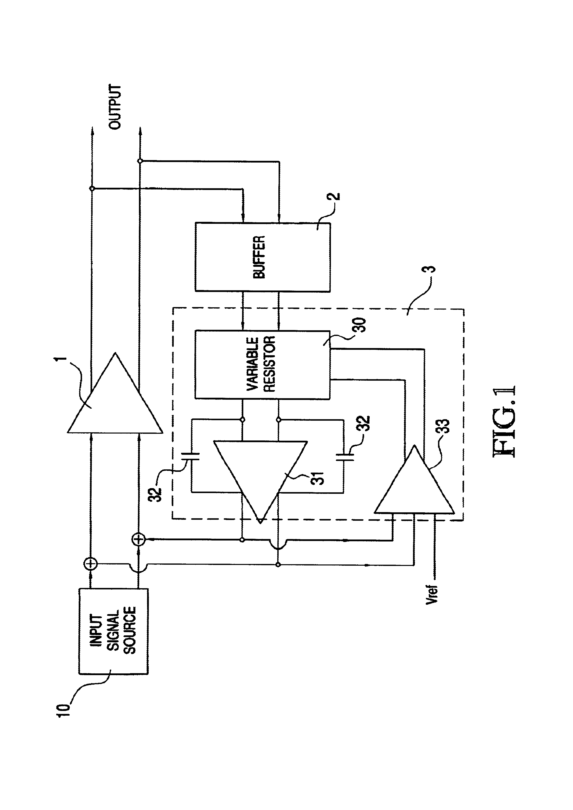
[0011]Refer to FIG. 1, a schematic circuit diagram of a gain amplifier with DC offset cancellation circuit is illustrated according to a preferred embodiment of the present invention. The gain amplifier comprises a gain amplifier, a buffer 2 and an active low-pass analogue filter 3. The gain amplifier 1 has an input end coupled to an input signal source 10. The buffer 2 has an input end coupled to the output end of the gain amplifier 1. The active low-pass analogue filter 3 is coupled to the output end of the buffer 2 for filtering input analog signals at high frequencies and providing a negative feedback by outputting filtered input analog signals to the input end of input signal source 10 to be deducted from the input signals, so as to cancel DC bias.

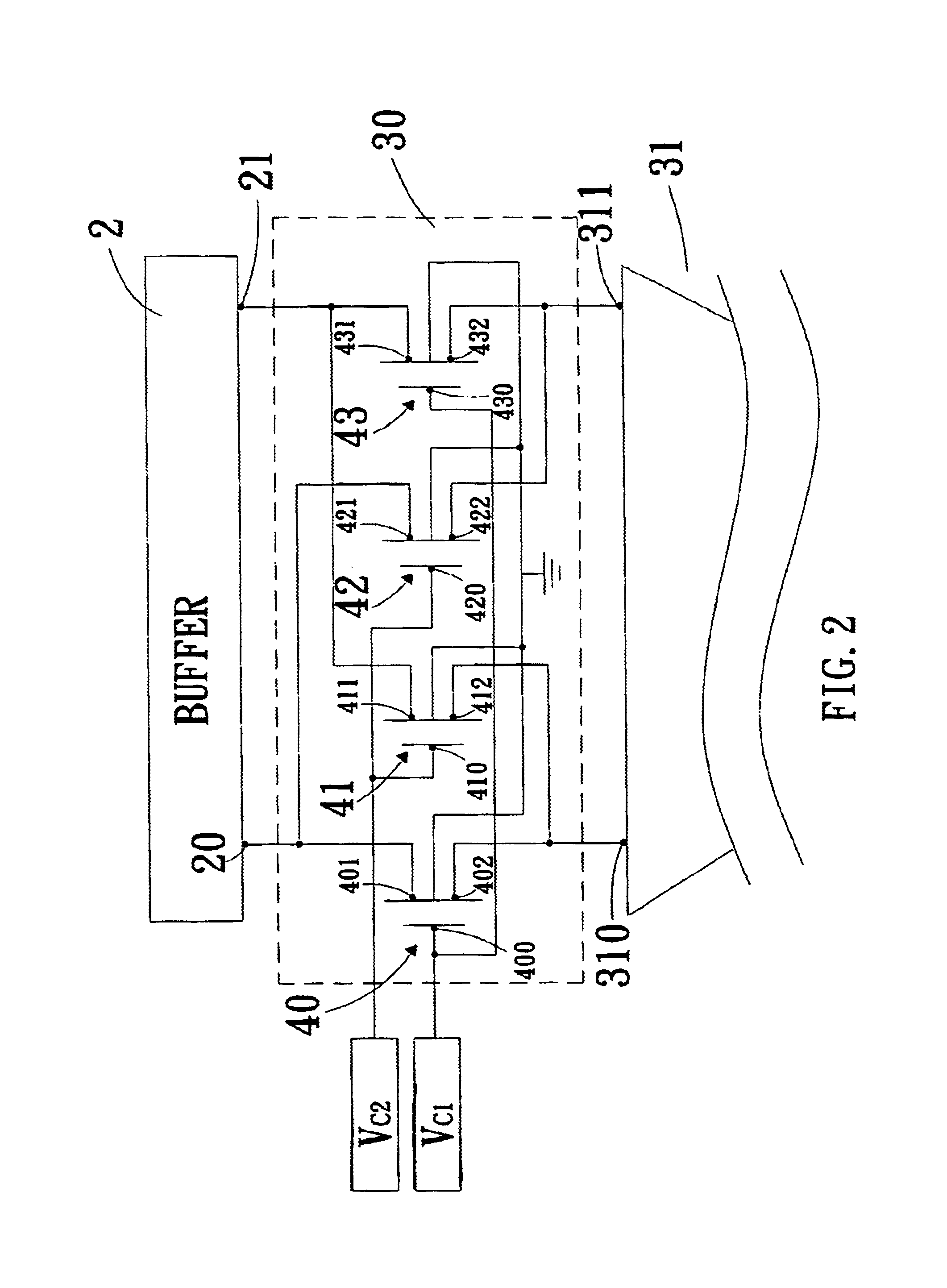
[0012]The active low-pass analogue filter 3 implemented in the preferred embodiment according to the present invention comprises: a variable resistor 30, an amplifier 31, a capacitor pair 32 and a comparator 33. The amplifier 31 is co...


PUM


Abstract

A DC offset cancellation circuit employs multiple feedback factors for canceling DC offset by increasing convergence time. The DC offset cancellation circuit features an active low-pass analogue filter including a variable resistor, an amplifier, a capacitor pair and a comparator, the amplifier being coupled to an output of the variable resistor. Negative feedback is provided from the output of the variable resistor to the input signal source, the capacitor pair is coupled to the amplifier, one input of the comparator is coupled to an output of the amplifier, and a second input of the comparator is coupled to a reference voltage source such that a comparison signal is output by the comparator to the variable resistor after comparing the negative feedback signal with a reference voltage.

Description

FIELD OF THE INVENTION[0001]The present invention relates generally to a gain amplifier with a DC offset cancellation circuit, and, more particularly, to a gain amplifier with DC offset cancellation circuit applied in digital communications systems.BACKGROUND OF THE INVENTION[0002]The programmable gain amplifier is an indispensable component in digital communications systems. A programmable gain amplifier is provided for boosting the gain of signals such that received input signals from radio frequency front-end circuits can be adjusted to a suitable level. Accordingly, by doing so, the demand for dynamic range of a base band analog-digital converter (ADC) is reduced. Moreover, if the input signal has a DC offset, a gain amplifier can be utilized for boosting the DC offset of the input current. After being processed by the gain amplifier, the resulting signals will saturate the following baseband ADC stage. As a result of coupling of the RF input to local oscillators, due to input o...

Claims


Application Information

Patent Timeline
IPC IPC(8): H03G1/00H03F3/45
CPCH03F3/45748H03G1/007H03F3/45973
Inventor WANG, CHAO-SHIUN
Owner IND TECH RES INST
Learn More