Fabrication of single crystal diamond tips and their arrays
a technology of diamond tips and diamond grains, which is applied in the direction of crystal growth process, polycrystalline material growth, after-treatment details, etc., can solve the problems of easy breakage of diamond coated silicon tips, distorted images, and frequent missing of diamond grains on tip apexes
- Summary
- Abstract
- Description
- Claims
- Application Information
AI Technical Summary
Benefits of technology
Problems solved by technology
Method used
Image
Examples
example
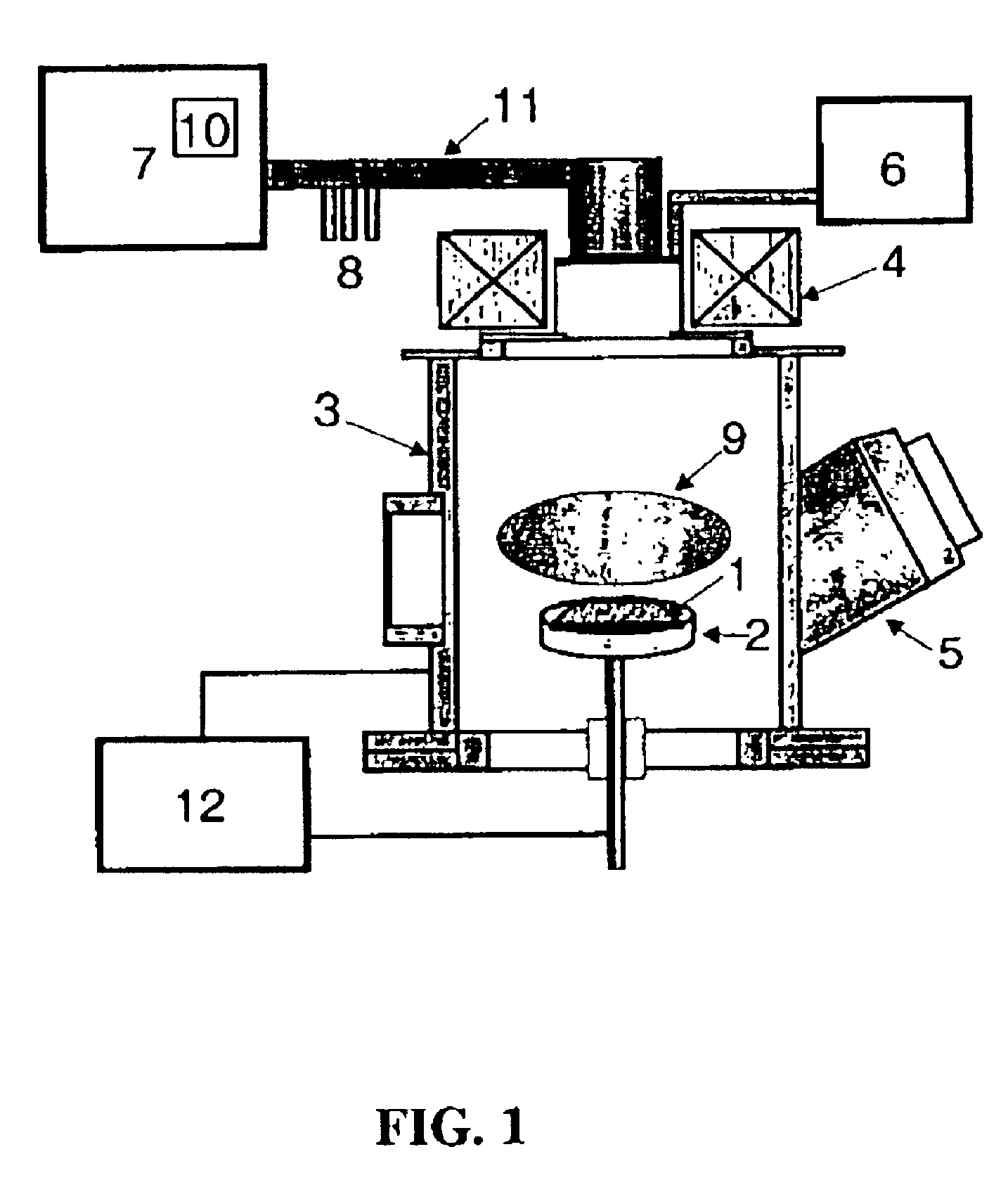
[0034]A textured [001] pyramidal-shaped diamond film, shown in FIG. 2 which is a SEM plain-view image, with a thickness of about 5 μm was prepared by microwave plasma CVD with controlled growth parameters such as concentration of carbon precursor and temperature using the CVD apparatus shown in FIG. 1.
[0035]The textured [001] pyramidal-shaped diamond film is subsequently etched in the same apparatus, but prior to etching of the oriented diamond film the reactor chamber was evacuated to 10−6 Torr by a turbo-molecular pump 5 and then hydrogen at a flow rate of 200 sccm was supplied into the chamber from a gas supply unit 6 to secure operation pressure of 40 Torr. 1500 W microwave power at 2.45 GHz supplied by a microwave generator 7 and fed via a waveguide 11 was applied to the hydrogen to form a microwave plasma. The reflected microwave power was adjusted to its minimum value, close to zero, using the impedance transformer 9. Both the forward and reflected microwave powers were const...
PUM
 Abstract
Description
Claims
Application Information
 - R&D
- Intellectual Property
- Life Sciences
- Materials
- Tech Scout
- Unparalleled Data Quality
- Higher Quality Content
- 60% Fewer Hallucinations
Browse by: Latest US Patents, China's latest patents, Technical Efficacy Thesaurus, Application Domain, Technology Topic, Popular Technical Reports.
© 2025 PatSnap. All rights reserved.Legal|Privacy policy|Modern Slavery Act Transparency Statement|Sitemap|About US| Contact US: help@patsnap.com


