Active element bias circuit for RF power transistor input

a technology of active element and gate bias voltage, which is applied in the direction of automatic tone/bandwidth control, high frequency amplifiers, and gain control, etc., can solve the problems of limited predistortion compensation ability to correct the distortion of the rf output signal caused by the variation in gate bias voltage in conventional rf amplifier circuits, and destroy the transistor device. , to achieve the effect of improving predistortion compensation and low impedan

Inactive Publication Date: 2005-05-17
TELEFON AB LM ERICSSON (PUBL)
View PDF15 Cites 4 Cited by
  • Summary
  • Abstract
  • Description
  • Claims
  • Application Information

AI Technical Summary

Benefits of technology

[0009]In one embodiment, the bias circuit includes an active element in series with a resistor in a DC bias circuit. The active element provides a relatively low impedance over a bandwidth comparable to an amplitude modulation bandwidth of the RF signal, such that a DC bias voltage applied at the active element has a fixed DC voltage at the resistor input, i.e., without any memory effect, thereby allowing for improved predistortion compensation.

Problems solved by technology

Since the gate of a GaAs FET is a Shottky barrier, the relatively strong RF input signal power will rectify the Shottky barrier and generate high positive gate current, which can destroy the transistor device.
As such, the ability of predistortion to correct the distortion of the RF output signal caused by the variation in the gate bias voltage in conventional RF amplifier circuits is limited.

Method used


Image

  • Active element bias circuit for RF power transistor input
  • Active element bias circuit for RF power transistor input
  • Active element bias circuit for RF power transistor input

Examples


Embodiment Construction

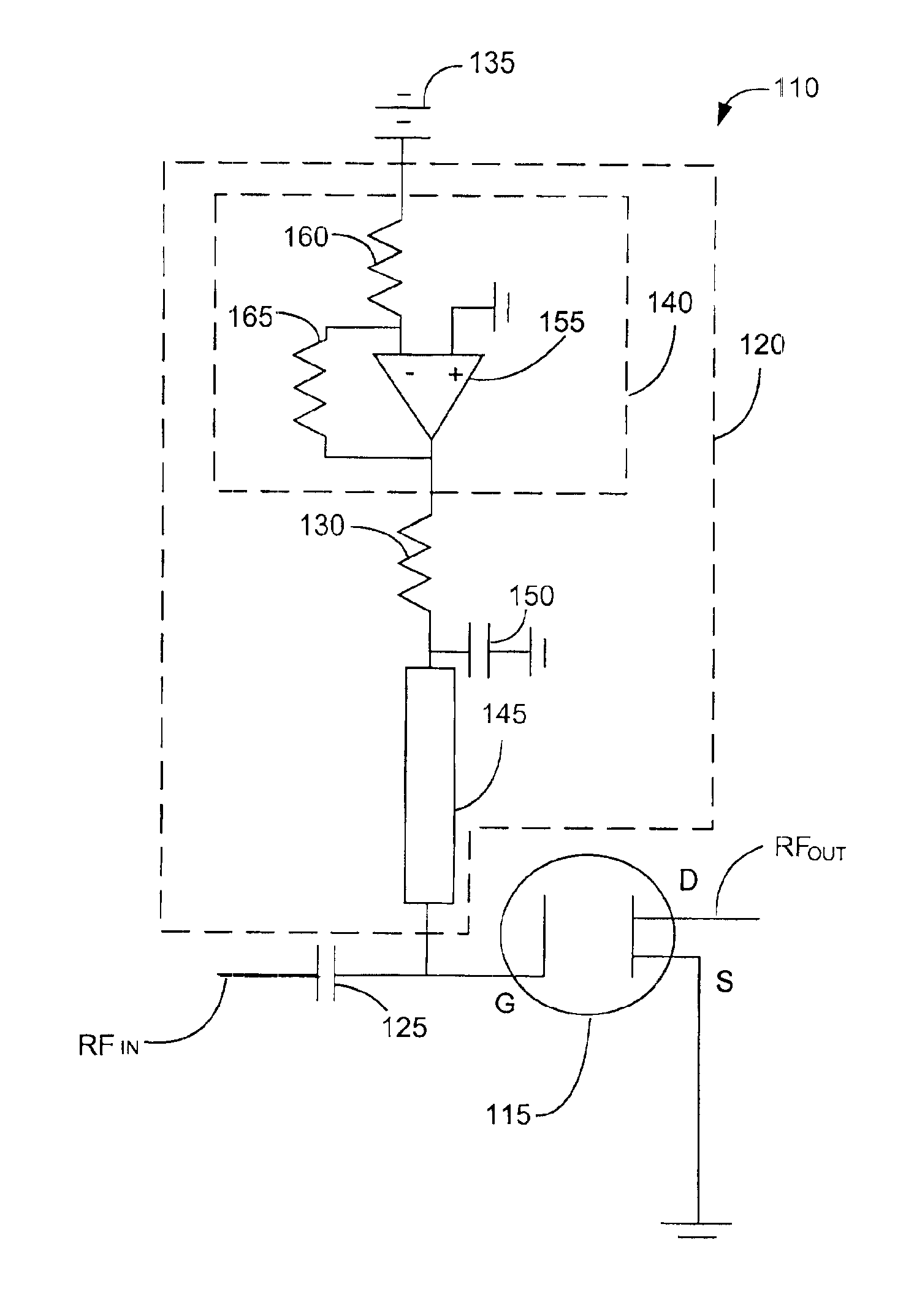
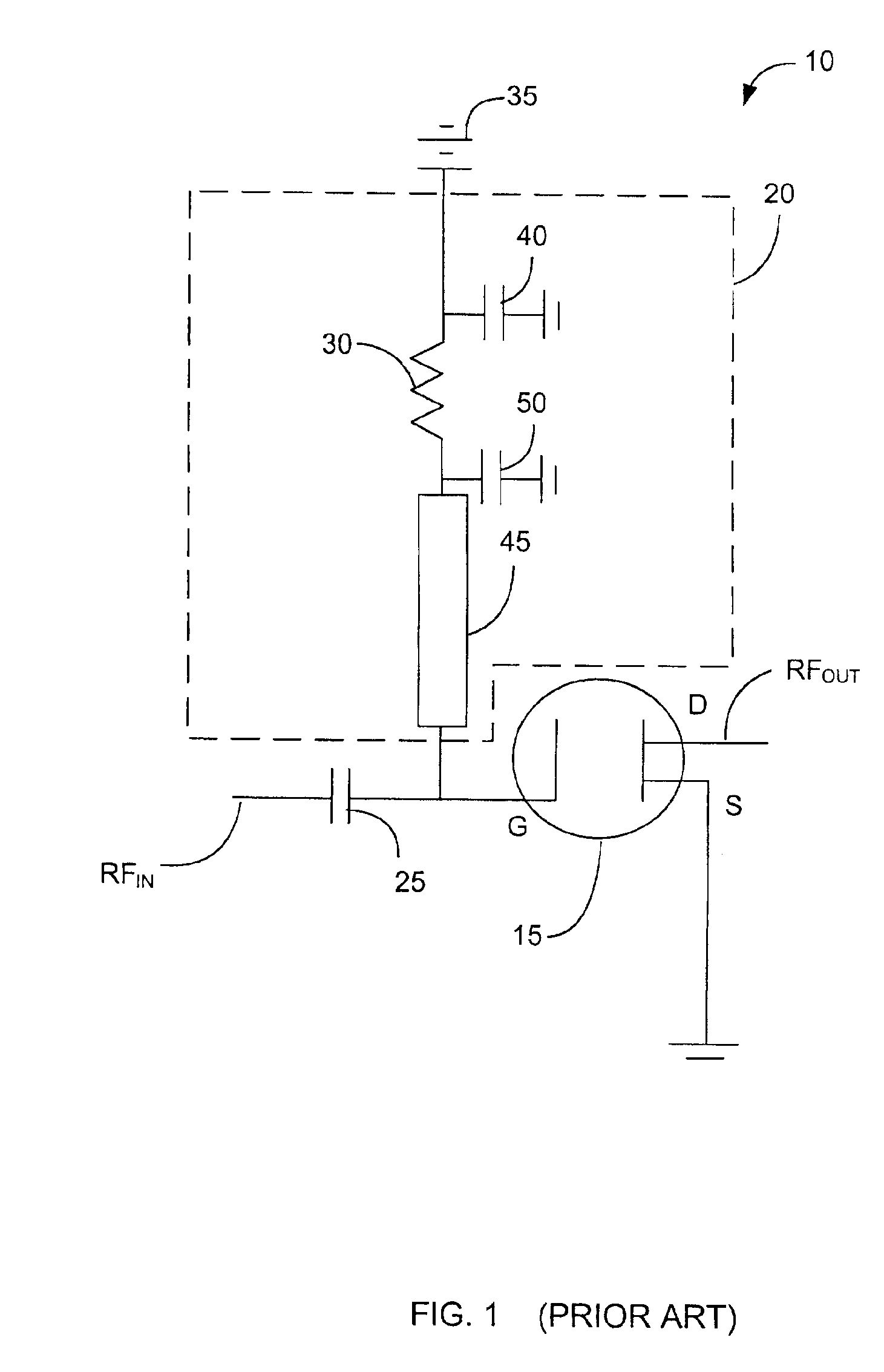
[0015]In accordance with the a general aspect of the invention, the passive capacitor used for providing a ground path for the gate current in conjunction with the current limiting resistor in conventional gate biasing circuits (e.g., capacitor 40 in the gate biasing circuit 20 of FIG. 1) is replaced with an active circuit element which provides a low output impedance over the operating frequency bandwidth of the RF input signal. In this manner, the gate current will see only a purely resistive load throughout the signal frequency bandwidth, without also further introducing unwanted memory effect into the biasing circuit.

[0016]Importantly, while the concepts and advantages of the invention will now be described in accordance with an embodiment directed to gate biasing of a GaAs FET, the invention may be equally employed in biasing circuits for other RF devices having drive dependent gate currents. By way of non-limiting examples, devices such as a GaAs pHEMT may also have drive depe...


PUM


Abstract

A biasing circuit for biasing a device (e.g., a GaAs field effect transistor) used for amplifying a radio frequency (RF) signal, the biasing circuit including an active element in series with a resistor, the active element providing a relatively low impedance over a bandwidth comparable to an amplitude modulation bandwidth of the RF signal, such that a DC bias voltage applied at the active element has a fixed DC voltage at the resistor input, i.e., without any memory effect, thereby allowing for improved predistortion compensation of non-linear voltage of the RF signal.

Description

FIELD OF THE INVENTION[0001]The present invention pertains generally to the field of radio frequency (RF) amplifier devices and, more specifically, to techniques for direct current (DC) biasing the input of a transistor used for amplifying a RF signal without incurring memory effect problems. By way of non-limiting example, the invention relates to RF power amplification circuits in wireless communication devices and networks.BACKGROUND OF THE INVENTION[0002]The use of transistor devices as signal amplifiers in wireless communication applications is well known. With the considerable recent growth in the demand for wireless services, such as personal communication services, the operating frequency of wireless networks has increased dramatically and is now well into the gigahertz (GHz) frequencies. At such high frequencies, Gallium Arsenide field effect transistors (GaAs FETs) have been preferred for power amplification applications, such as, e.g., use in mobile communication devices ...

Claims


Application Information

Patent Timeline
IPC IPC(8): H03F3/189H03F1/30H03F3/193
CPCH03F3/193H03F1/30
Inventor MARRA, THOMASMATHE, LENNART
Owner TELEFON AB LM ERICSSON (PUBL)
Why Eureka
Try Eureka