
Method, memory system and memory module board for avoiding local incoordination of impedance around memory chips on the memory system

a technology of memory system and impedance, applied in the direction of electrical digital data processing, instruments, logic circuits, etc., can solve the problems of incoordination of impedance around the dram chip, exercise harmful influence on the frequency response of the data bus, etc., and achieve the effect of avoiding local incoordination of impedance around memory

Inactive Publication Date: 2005-04-19
LONGITUDE LICENSING LTD
View PDF11 Cites 23 Cited by
  • Summary
  • Abstract
  • Description
  • Claims
  • Application Information

AI Technical Summary

Benefits of technology

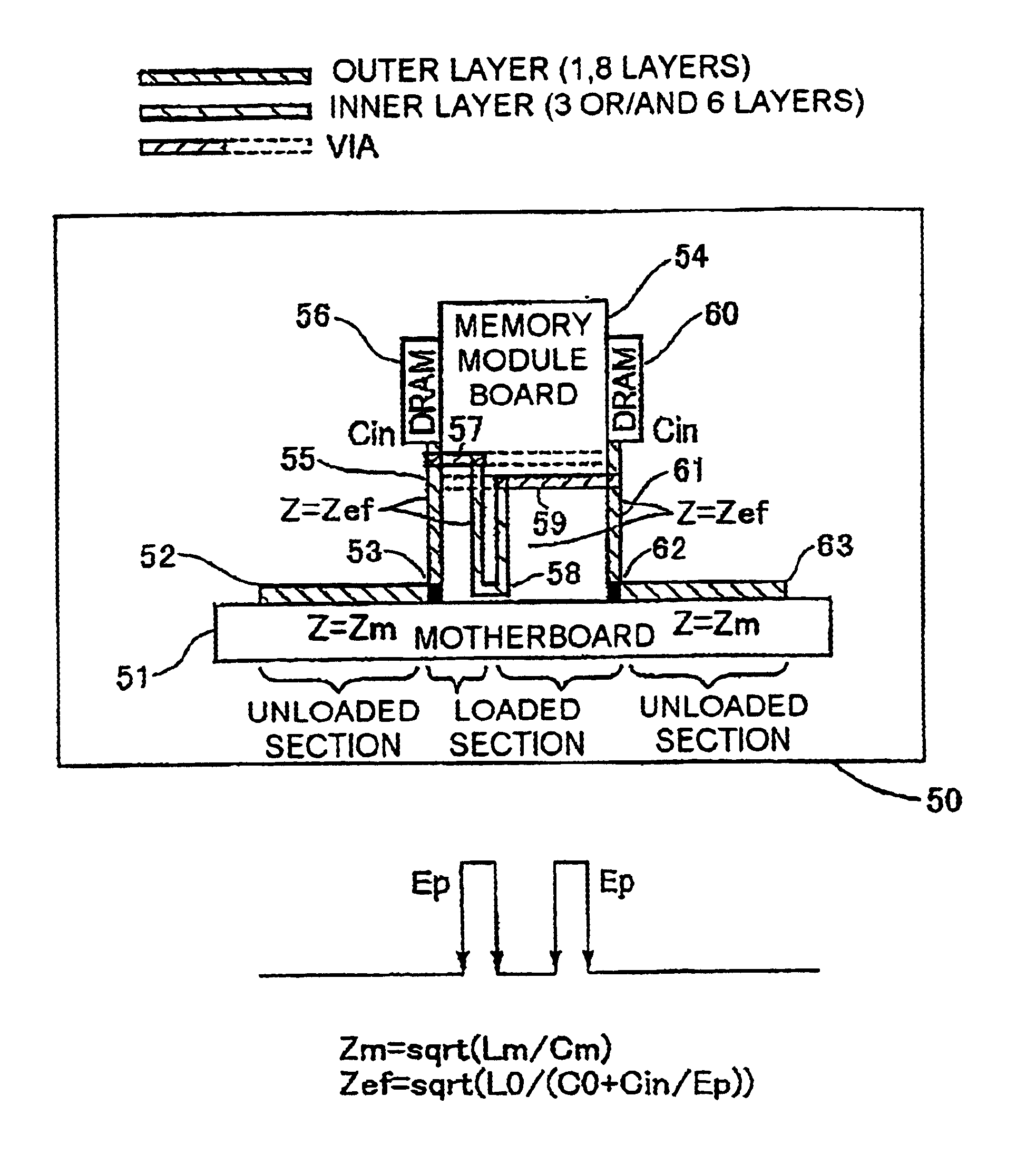
[0065]As mentioned above, according to the present invention, impedance of wire nearby circuit elements with additional capacitance cancels decrement of impedance caused by the additional capacitance. Therefore, the present invention can avoid local incoordination of impedance in a data bus and, as a result, can improve frequency response of the data bus.
[0066]For example, when the present invention is adopted to a memory bus of a personal computer, decrement of impedance caused by additional capacitance of DRAM chips can be canceled by the wire on a memory module board on which the DRAM chips are mounted. This cancellation is made by adjusting length, width and / or thickness of the wire.

Problems solved by technology

Additional capacitance causes incoordination of impedance around the DRAM chip.
The incoordination of impedance causes signal reflection and, exercises a harmful influence on frequency response of the data bus.

Method used


Image

  • Method, memory system and memory module board for avoiding local incoordination of impedance around memory chips on the memory system
  • Method, memory system and memory module board for avoiding local incoordination of impedance around memory chips on the memory system
  • Method, memory system and memory module board for avoiding local incoordination of impedance around memory chips on the memory system

Examples


Embodiment Construction

[0034]Description will be made about a data bus system 1, which is suitable for the present invention. As shown in FIG. 4A, in a data bus system 1, each of eight DQ lines 3 wired on a motherboard 2 is connected via two memory module boards 4 and 5 to a terminal resistance 6. Each of CMD / ADD lines 7 is connected to CMD / ADD registers 8 on the memory module boards 4 and 5. As shown in FIG. 4B, DQ lines 3 are stubless-wired. Namely, a DQ line 3 running from a chipset 9 is wired through lead pins of DRAM chips 11 and 12 on the memory module 4 and DRAM chips 13 and 14 on the memory module 5 to the terminal resistance 6, as if the DQ line 3 were drawn without lifting pen from paper.

[0035]Generally, a DRAM chip has additional capacitance, and consequently, causes a decrease in impedance. According to the present invention, the decrease in impedance is canceled by the impedance of the wire on a memory module board. As a result, impedance of a motherboard and impedance of a memory module boar...


PUM


Abstract

A signal line of a data bus includes first wires on a first board and a second wire on a second board. The second board is installed on the first board to connect the first and second wires with each other in series to establish the signal line. Semiconductor devices are connected with the second wire. In such data bus system, impedance of the second wire is decided according to additional capacitance of the semiconductor device on the second board in order to harmonize impedance of the first board with impedance of the second board.

Description

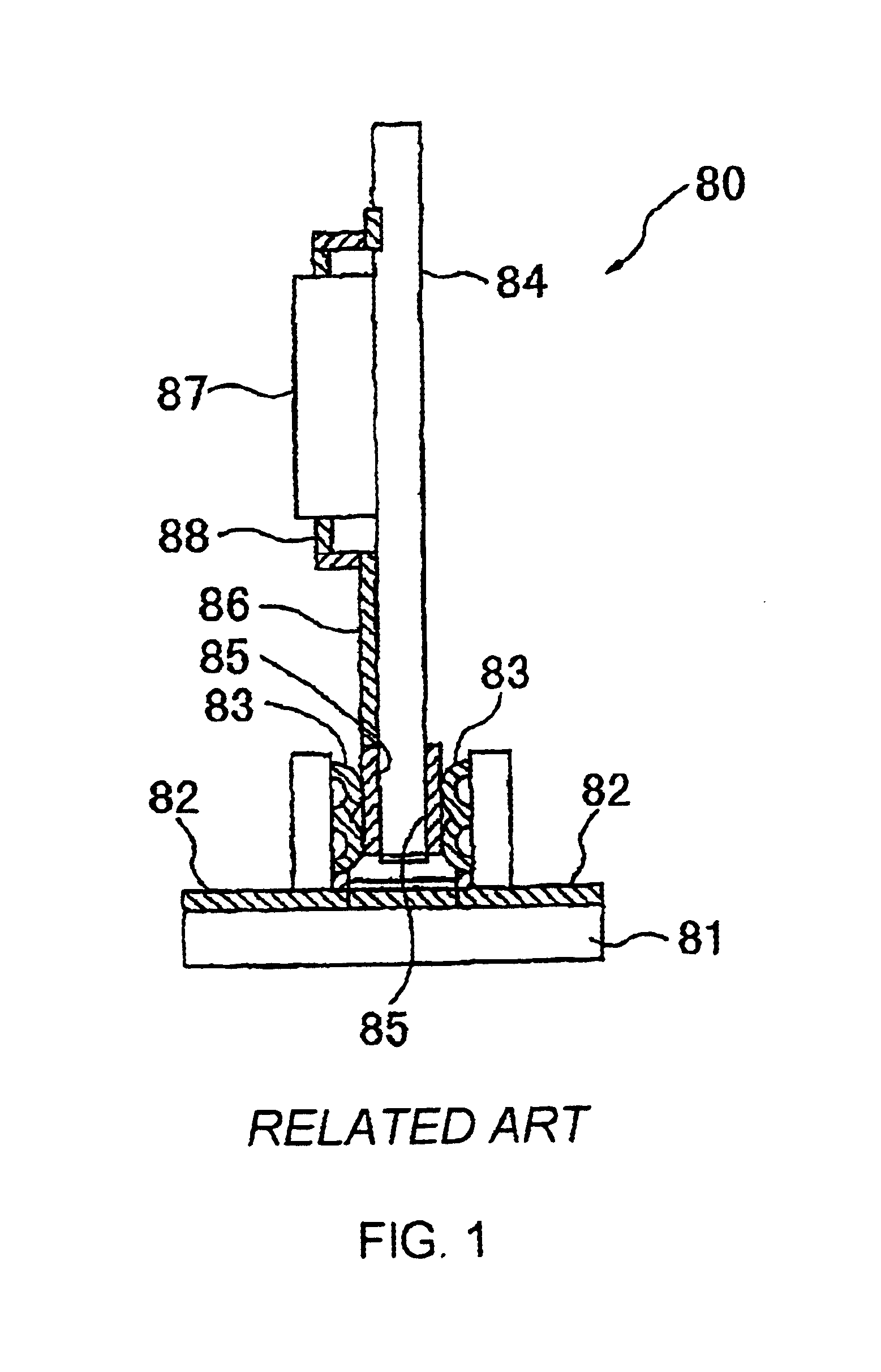
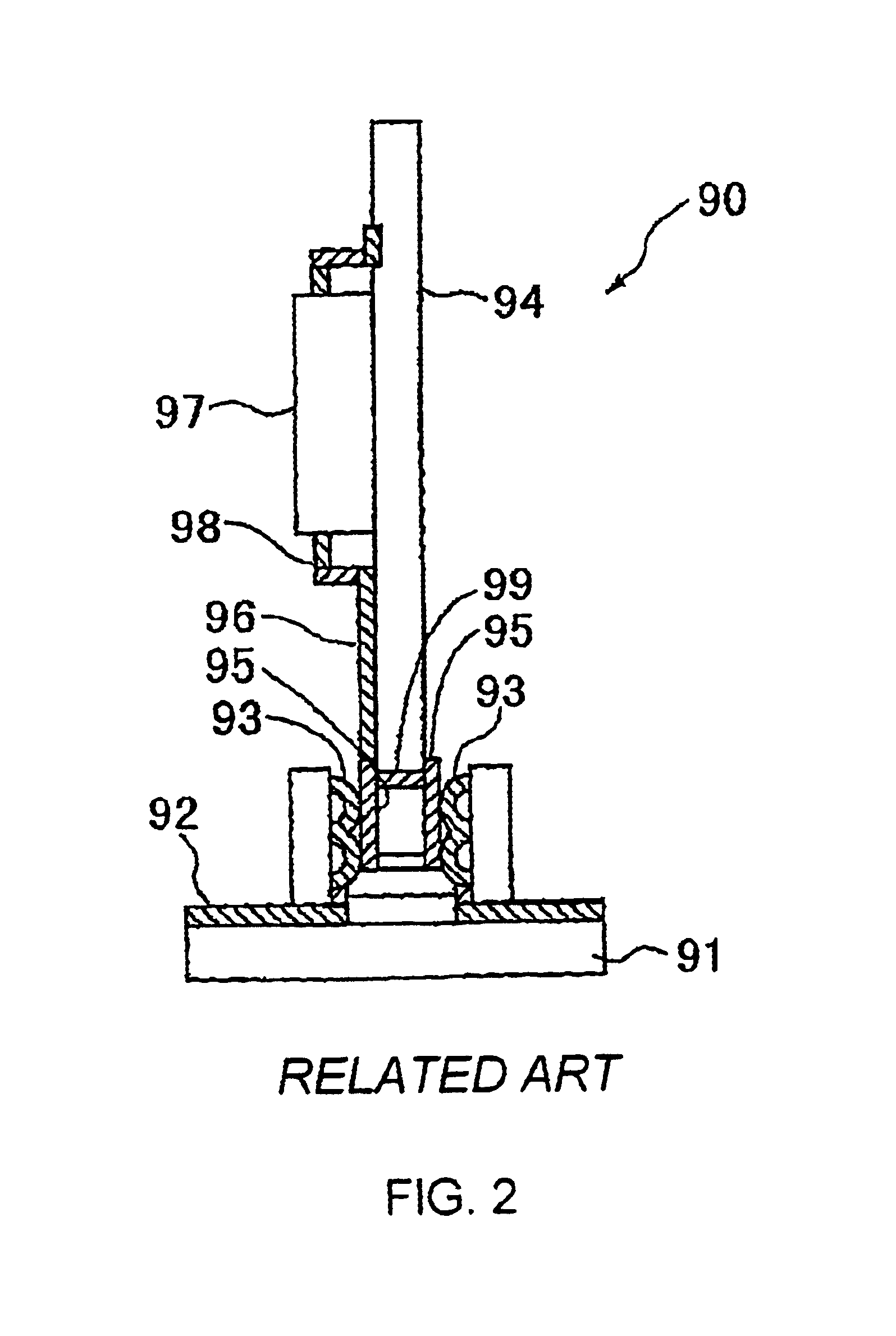
BACKGROUND OF THE INVENTION[0001]This invention relates to wiring of a data bus and, in particular, wire structure of a data bus on a motherboard and a memory module board plugged into a connector on the motherboard. Typically, a personal computer includes a motherboard and memory module boards.[0002]In recent years, the processing speed of a CPU (central processing unit) has accelerated, and as a result, it is required that the frequency response of a data bus becomes faster. In this specification, it is assumed that the frequency response of a data bus is over 100 MHz.[0003]In a conventional data bus of a personal computer, the T-stub wiring structure shown in FIG. 1 is adopted for branching bus lines and control lines for DRAM (dynamic random-access memory). The following describes a memory module 80 with the T-stub wiring structure with reference to FIG. 1.[0004]A connector 83 is installed on a bus line 82 wired on a main board 81. A memory module board 84 is plugged into the co...

Claims


Application Information

Patent Timeline
Patent Type & Authority Patents(United States)
IPC IPC(8): G11C5/06G11C5/00H05K1/14H05K1/02G06F12/00G06F13/16G06F3/00H01L27/10
CPCG11C5/063H05K1/14H05K1/0237H01L2924/0002H01L2924/00H01L27/10
Inventor ABO, HISASHIIKEDA, HIROAKI
Owner LONGITUDE LICENSING LTD
Learn More