Optical delay line and manufacturing method therefor
a technology of optical delay line and manufacturing method, which is applied in the direction of manufacturing tools, cladding optical fibre, instruments, etc., can solve the problems of difficult to realize the element at a low cost, difficult to make a transmission type element, and scarcely a practical means to meet this need. , to achieve the effect of accurately and uniformly machining a large area of cladding, accurate control of position
- Summary
- Abstract
- Description
- Claims
- Application Information
AI Technical Summary
Benefits of technology
Problems solved by technology
Method used
Image
Examples
embodiment 1
(Embodiment 1)
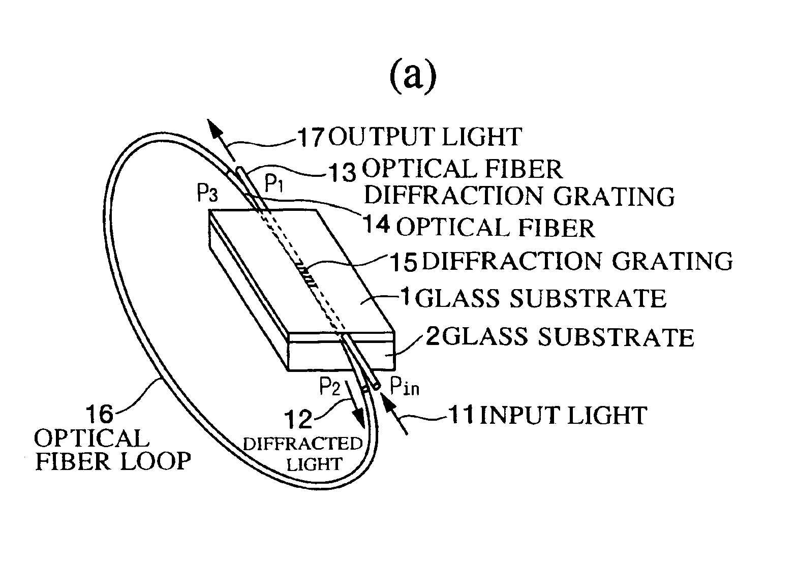
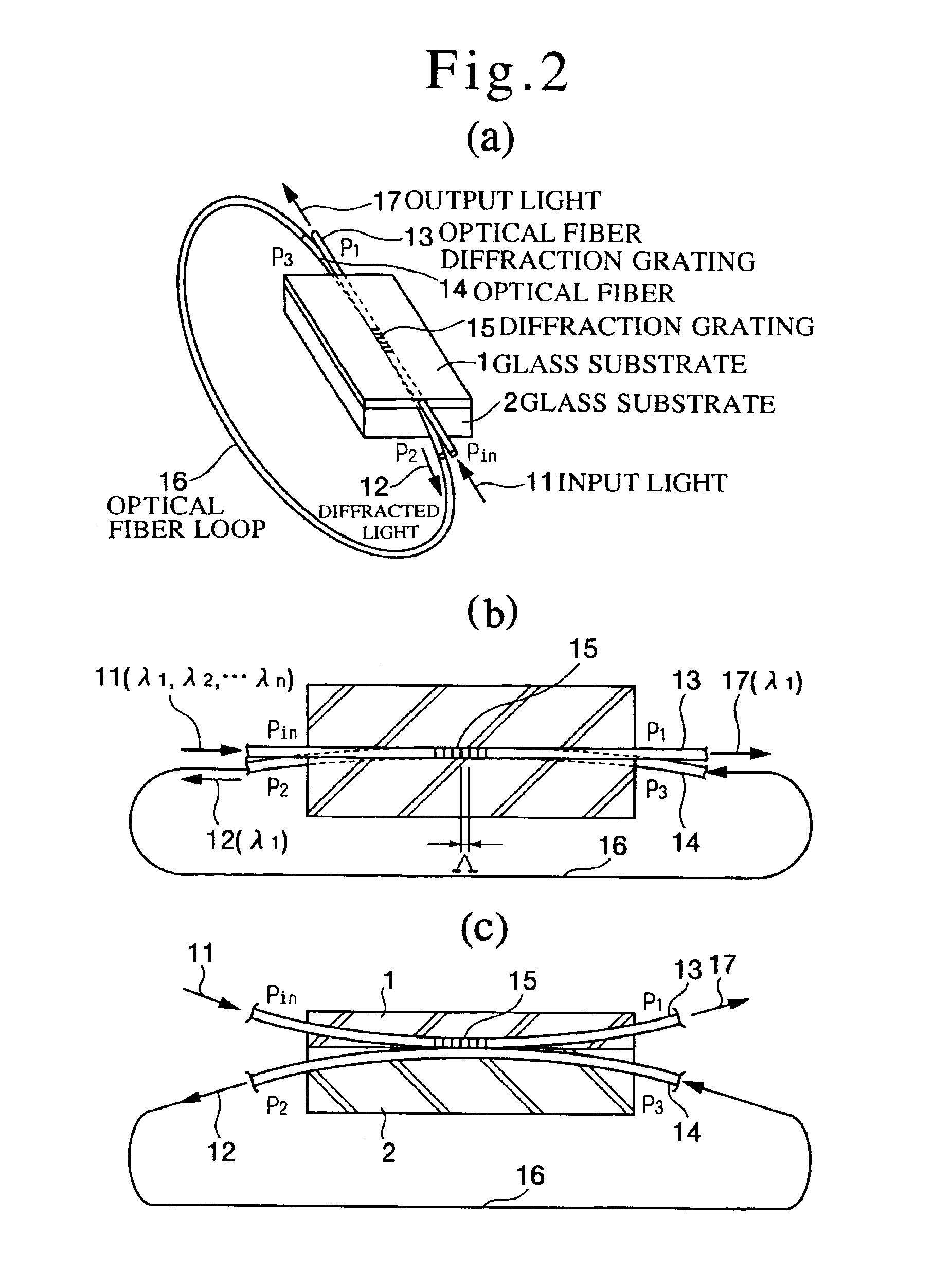
Preferred embodiments of the present invention will be described below with reference to accompanying drawings. FIG. 2 schematically shows the configuration of an optical delay line in Embodiment 1 of the invention, in which FIG. 2(a) is an overall perspective view of the optical delay line; FIG. 2(b), a plan of its directional coupler portion; and FIG. 2(c), a profile of its directional coupler portion. Reference numerals 1 and 2 denote glass substrates; 11 denotes an input light; 12 denotes an diffracted light; 13 denotes an optical fiber diffraction grating; 14 denotes an optical fiber; 15 denotes a diffraction grating formed in the optical fiber diffraction grating 13; 16 denotes an optical fiber loop for giving a delay; and 17 denotes an output light.
The operation of the optical delay line configured as described above will now be described. The input light 11 having a plurality of wavelength components (λ1, λ2, . . . λn) is brought to incidence on the optical fib...
embodiment 2
(Embodiment 2)
Next will be described Embodiment 2 of the present invention with reference to FIG. 3 and FIG. 4. FIG. 3 schematically shows an overall configuration of an optical delay line having two diffraction gratings differing in refractive index modulation pitch, wherein reference numerals 1 and 2 denote glass substrates; 21 denotes an input light; 22 denotes an diffracted light; 23 denotes an optical fiber diffraction grating; 24 denotes an optical fiber; 25 and 26 denote a first diffraction grating and a second diffraction grating, respectively, formed in the optical fiber diffraction grating 23; 27 denotes an optical fiber loop for generating a delay; and 28 denotes an output light. FIG. 4(a) shows the spectrum of the input light 21 in a case where an actually fabricated element is used, and FIG. 4(b), the spectrum of the diffracted light 22. A super-luminescent diode is used as the source of the input light 21, having a wideband spectral characteristic of 100 nm or more. Th...
embodiment 3
(Embodiment 3)
Next will be described Embodiment 3 of the present invention with reference to FIG. 5 and FIG. 6. FIG. 5 schematically shows an overall configuration of an optical delay line having four diffraction gratings differing in refractive index modulation pitch, wherein reference numerals 1 and 2 denote glass substrates; 41 denotes an input light; 42 denotes an diffracted light; 43 denotes an optical fiber diffraction grating; 44 denotes an optical fiber; 45, 46, 47 and 48 denote a first diffraction grating, a second diffraction grating, a third diffraction grating and a fourth diffraction grating, respectively, formed in the optical fiber diffraction grating 43; 49 denotes an optical fiber loop for generating a delay; and 50 denotes an output light. FIG. 6(a) shows the spectrum of the input light 41 in a case where an actually fabricated element is used, and FIG. 6(b), the spectrum of the diffracted light 42. A super-luminescent diode is used as the source of the input light...
PUM
| Property | Measurement | Unit |
|---|---|---|
| refractive index | aaaaa | aaaaa |
| time delay | aaaaa | aaaaa |
| specific wavelength | aaaaa | aaaaa |
Abstract
Description
Claims
Application Information
 - R&D
- Intellectual Property
- Life Sciences
- Materials
- Tech Scout
- Unparalleled Data Quality
- Higher Quality Content
- 60% Fewer Hallucinations
Browse by: Latest US Patents, China's latest patents, Technical Efficacy Thesaurus, Application Domain, Technology Topic, Popular Technical Reports.
© 2025 PatSnap. All rights reserved.Legal|Privacy policy|Modern Slavery Act Transparency Statement|Sitemap|About US| Contact US: help@patsnap.com


