Temperature-protected semiconductor switch

a semiconductor switch and temperature protection technology, applied in the direction of electronic switching, emergency protective circuit arrangement, pulse technique, etc., can solve the problems of temperature sensor a relatively large distance from the hottest location, charge carrier diffusion rings, and other problems, to achieve the effect of simple semiconductor switch layou

Inactive Publication Date: 2005-04-05
INFINEON TECH AG
View PDF10 Cites 15 Cited by
  • Summary
  • Abstract
  • Description
  • Claims
  • Application Information

AI Technical Summary

Benefits of technology

In an embodiment, the charge carrier detector is arranged neighboring the temperature sensor which is, in turn, applied in the proximity of the hottest location of the semiconductor switch. Ideally, the charge carrier detector is arranged neighboring a signal line of the temperature sensor that leads out of the semiconductor switch. In this case, a signal line of the charge carrier detector can be conducted out of the semiconductor switch spatially adjacent to the signal line of the temperature sensor. A particularly simple layout of the semiconductor switch is thus possible since only a few modifications need be undertaken compared to a semiconductor switch known from the prior art.

Problems solved by technology

When the temperature sensor together with the semiconductor switch element is integrated in a semiconductor body, the technologically integrated diode can present problems for the semiconductor switch element from source to drain.
The charge carrier diffusion rings, which are also referred to as “suction rings”, however, have only a limited effect given high currents through the integrated reverse diode.
This, however, would have the disadvantageous effect that the temperature sensor exhibits a relatively great distance from the hottest location of the semiconductor switch element.
When, on the other hand, the charge carrier diffusion is implemented too low, this cannot adequately efficiently protect the temperature sensor given extremely high currents through the reverse diode D1 in order to prevent the undesired, parasitic effects to the temperature sensor.

Method used


Image

  • Temperature-protected semiconductor switch
  • Temperature-protected semiconductor switch
  • Temperature-protected semiconductor switch

Examples


Embodiment Construction

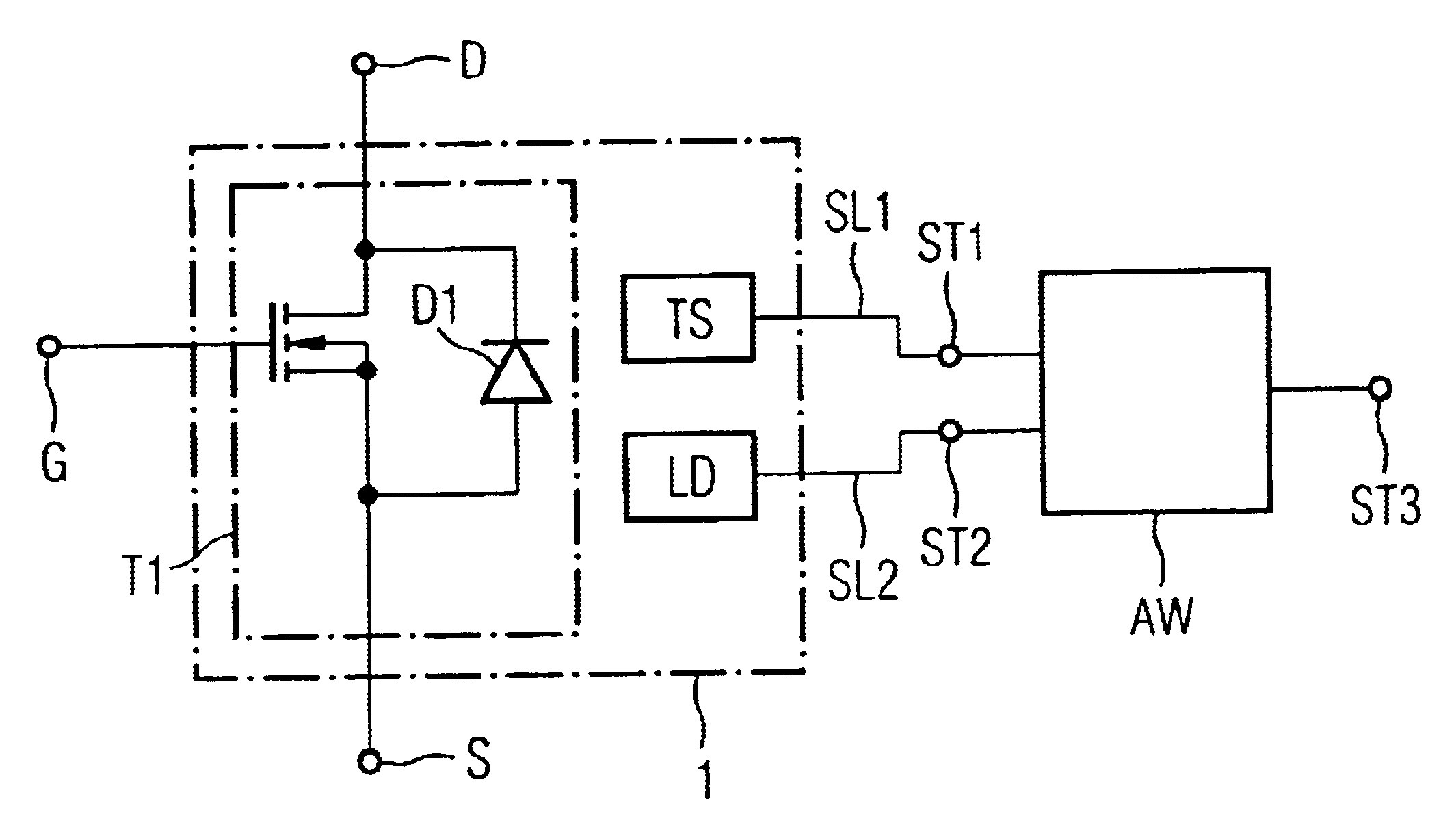
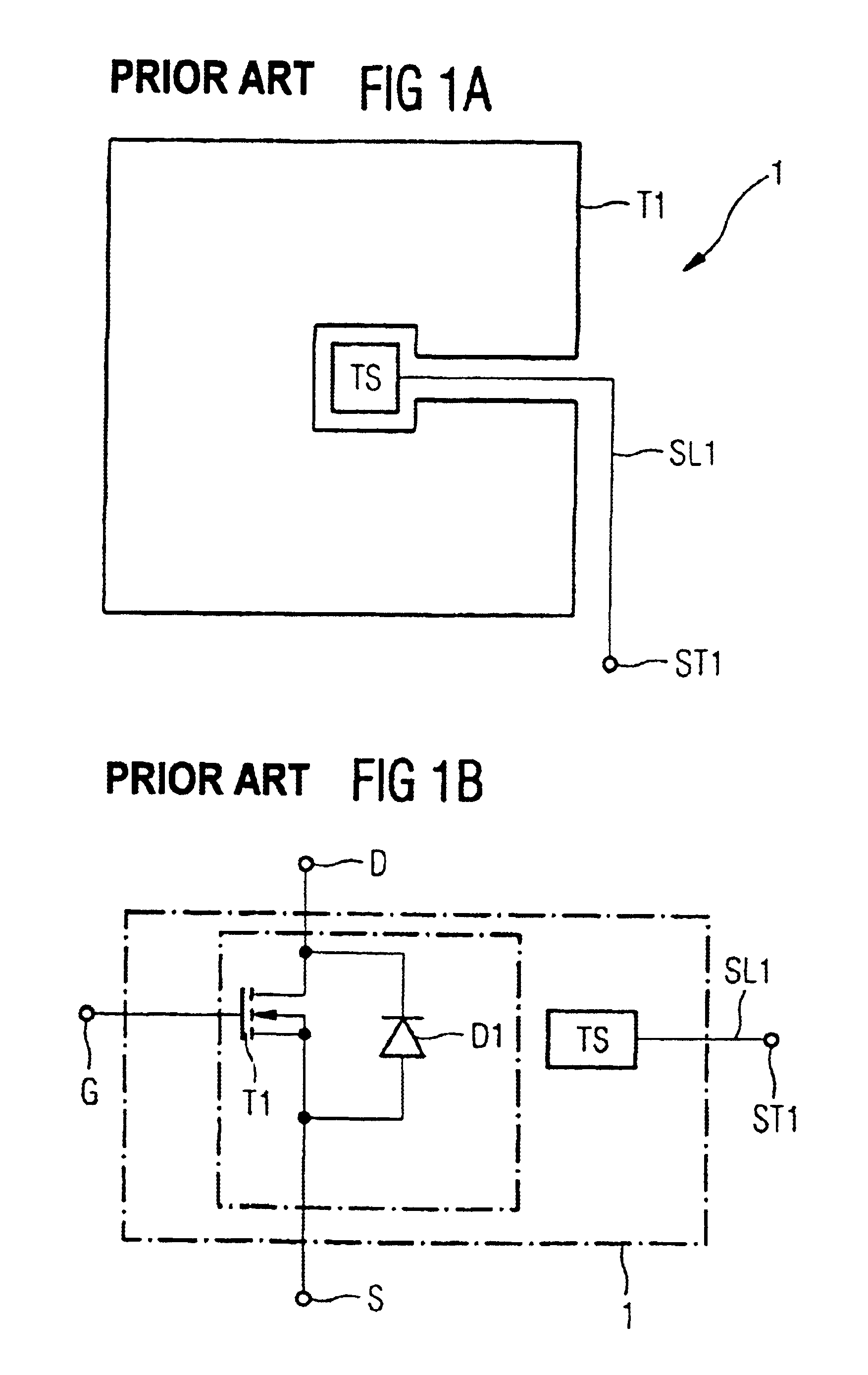
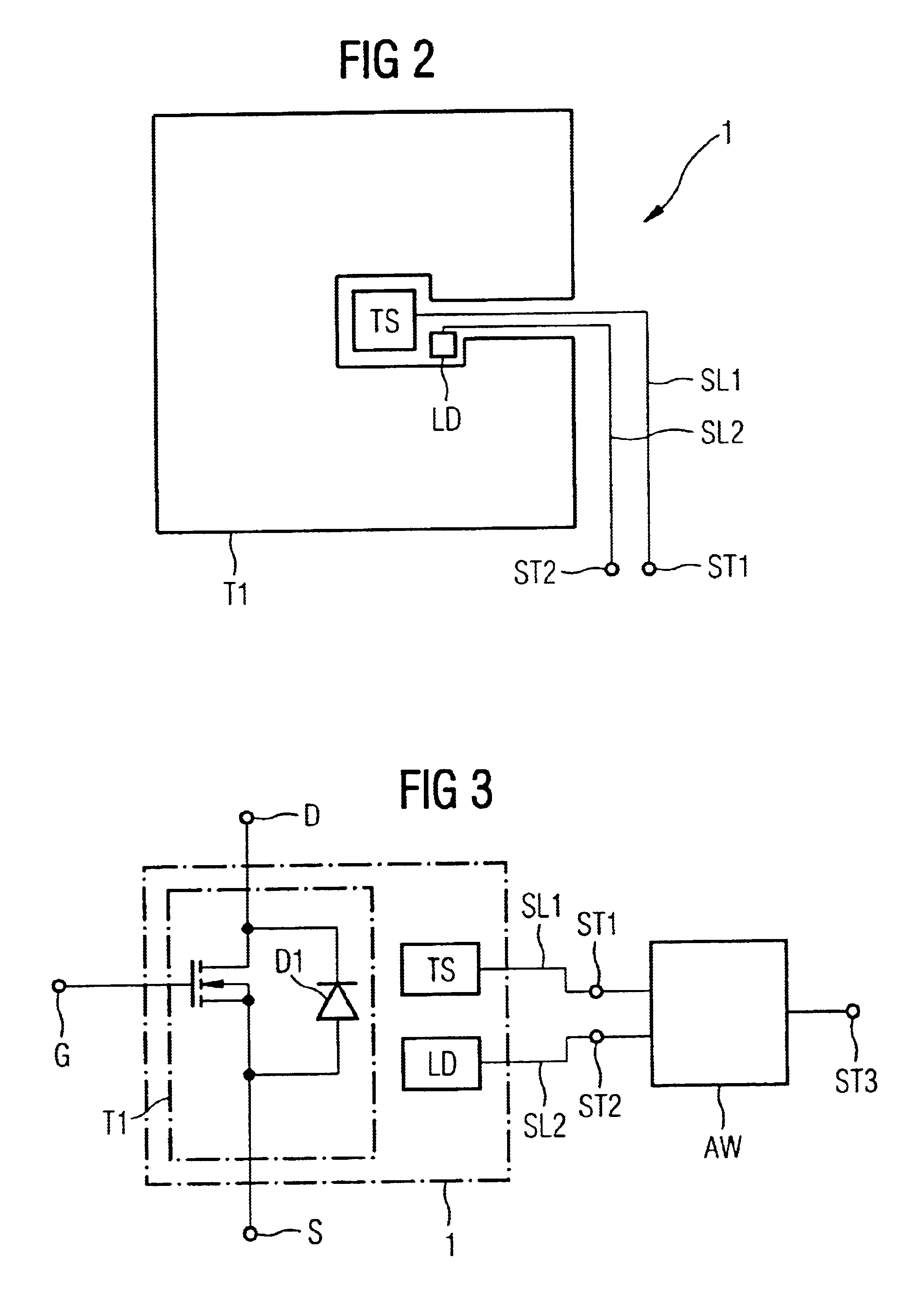
FIG. 2 shows a schematic plan view onto the inventive, temperature-protected semiconductor switch 1. This is composed of a semiconductor switch element T1 that is, in turn, composed of a number of MOS cells (not shown) connected in parallel. A temperature sensor TS is attached in the proximity to the hottest location of the semiconductor switch element TS1, the temperature sensor TS outputting a signal via a signal line SL1 to a status output ST1 when a predetermined temperature threshold is upwardly exceeded. A charge carrier detector LD is arranged neighboring the temperature sensor TS, this detector LD likewise including a signal line SL2 that is connected to a status output ST2. The charge carrier detector LD is thereby arranged neighboring the temperature sensor TS, whereby the preferred location exists close to the junction of the signal line SL1 and the temperature sensor TS. The charge carrier detector LD, of course, could be arranged at any arbitrary location in the semicon...


PUM


Abstract

A temperature-protected semiconductor switch having a semiconductor switch element composed of a number of cells connected in parallel and an integrated reverse diode, and further having a temperature sensor wherein the semiconductor switch element and the temperature sensor are integrated together in a semiconductor body of a first conductivity type. Upon occurrence of an excess temperature, the temperature sensor generates a first signal. A charge carrier detector is also provided which generates a second signal given the occurrence of free charged carriers caused by the integrated reverse diode in the semiconductor body. The first and second signals are supplied to an evaluation means that, for examples, undertakes the shut-off of the semiconductor switch only in the case of a true excess temperature.

Description

BACKGROUND OF THE INVENTION1. Field of the InventionThe present invention is directed to a temperature-protected semiconductor switch having a semiconductor switch element which is composed of a number of cells connected in parallel and which includes an integrated reverse diode. The temperature-protected semiconductor switch also has a temperature sensor wherein the semiconductor switch element and the temperature sensor are integrated together in a semiconductor body of a first conductivity type and wherein the temperature sensor generates a first signal given the occurrence of an excessive temperature.2. Description of the Prior ArtFor protection against thermal overload, semiconductor switches, particularly power switches, are provided with integrated temperature sensors. The temperature sensors acquire the temperature of the power switch and convert this into a temperature-dependent, analog signal which then can be interpreted in a circuit. As a result thereof, for example, a s...

Claims


Application Information

Patent Timeline
Patent Type & Authority Patents(United States)
IPC IPC(8): H01L27/02H02H5/00H02H5/04H03K17/082H03K17/08
CPCH01L27/0248H02H5/044H03K17/0822H03K2017/0806H01L2924/0002H01L2924/00
Inventor SANDER, RAINALD
Owner INFINEON TECH AG
Why Eureka
Try Eureka