CPP spin valve head with bias point control
- Summary
- Abstract
- Description
- Claims
- Application Information
AI Technical Summary
Benefits of technology
Problems solved by technology
Method used
Image


Examples
first embodiment
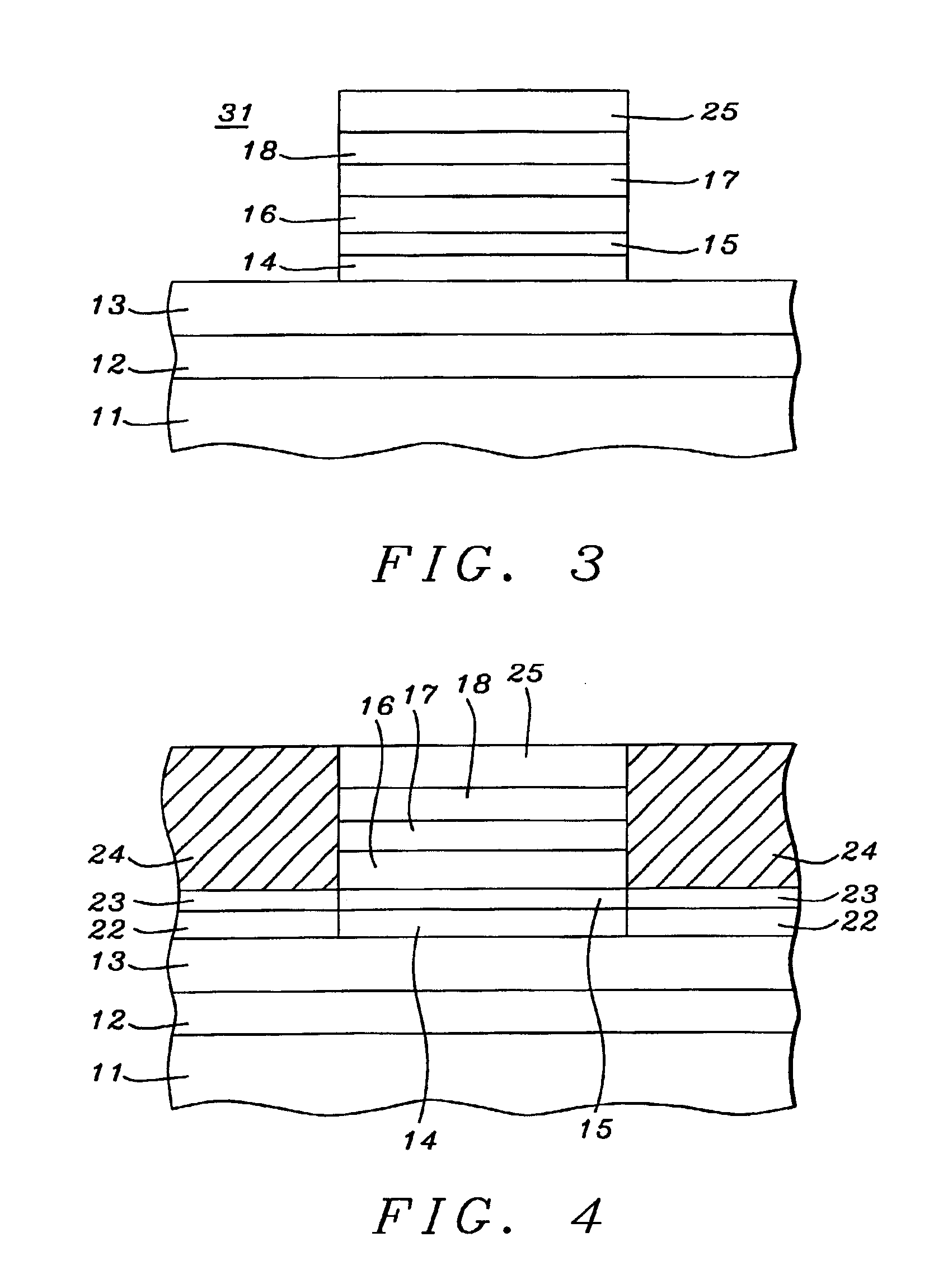
A schematic drawing of the first embodiment is shown in FIG. 5. In this scheme, the bottom AFM layer 12 is used to help the bias point control. The synthetic pattern exchange layer 22 / 23 at the side wings of free layer 13 provides a stabilization scheme for the free layer. The synthetic pinning at the side region can significantly reduce the current induced circular field effect, thereby enabling large current input. No current leakage occurs since the Cu layer is patterned. Transverse pinning of the AP layer is more relaxed compared to that in the second prior art design since the AP layer shape anisotropy is much smaller than in the previous case. Also, due to the pinning of the free layer side wings, the required bottom AFM pinning strength can then be reduced compared to that of the first design.
All of the above designs have some degree of bias point control problems since none of them has another transverse field to cancel the stray field from the AP layer: The design shown in ...
second embodiment
We refer now to FIG. 6 for a description of the invention which was mentioned earlier. The process and structure are similar to that seen in FIG. 5 except that, the bottom antiferromagnetic layer (layer 12), is replaced by a second spin valve. This second spin valve is, in effect, a mirror reflection of layers 14 through 17.
Thus, bottom antiferromagnetic layer 68 is deposited onto lower conductive magnetic shield 11, whose conductance is enhanced by a layer of copper and / or gold and which is between about 100 and 300 Angstroms thick. This is followed by a ferromagnetic layer which is then magnetized in a first direction to become AP4 layer 65. AP4 is between about 10 and 30 Angstroms thick and is of CoFe, Co, or CoFeB. Then antiferromagnetic coupling layer 66 (between about 3 and 10 Angstroms thick and of Ru or Rh) is deposited on AP4 layer 65, followed by another ferromagnetic layer which is then magnetized in a second direction, antiparallel to the first direction, to become AP3 l...
PUM
 Abstract
Description
Claims
Application Information
 - R&D
- Intellectual Property
- Life Sciences
- Materials
- Tech Scout
- Unparalleled Data Quality
- Higher Quality Content
- 60% Fewer Hallucinations
Browse by: Latest US Patents, China's latest patents, Technical Efficacy Thesaurus, Application Domain, Technology Topic, Popular Technical Reports.
© 2025 PatSnap. All rights reserved.Legal|Privacy policy|Modern Slavery Act Transparency Statement|Sitemap|About US| Contact US: help@patsnap.com