
Bi-directional impedance matching circuit

a bi-directional impedance matching and integrated circuit technology, applied in logic circuit coupling/interface arrangement, pulse technique, baseband system details, etc., can solve the problems of poor signal integrity of transmitted signals, poor signal integrity of received signals, impedance mismatch between terminating or input impedances, etc., to achieve accurate impedance matching, low power mode, and good or high signal integrity

Inactive Publication Date: 2005-02-01
AVAGO TECH INT SALES PTE LTD
View PDF3 Cites 7 Cited by
  • Summary
  • Abstract
  • Description
  • Claims
  • Application Information

AI Technical Summary

Benefits of technology

The impedance or resistance values of the first switchable impedance and the second switchable impedance are selected to appropriately match the impedance of a selected channel, such as a 50 Ohm channel impedance. As a consequence, use of the present invention in high speed buffers or other input and output circuitry preserves good or high signal integrity of both a transmitted signal and a received signal, due to providing accurate impedance matching between the output impedance, the input impedance, and the channel impedance. The present invention also may be embodied as an integrated circuit. In addition, the present invention provides a low power mode, to avoid power dissipation through the switchable impedances when not in use.

Problems solved by technology

In some cases, use of such high speed buffers often results in poor signal integrity of the transmitted signal due to an impedance mismatch between the high speed buffer output impedance (“RO”) and the channel impedance (“ZO”).
In other cases, poor signal integrity of a received signal often results from an impedance mismatch between the terminating or input impedance (“RT”) (present at the PAD or other interface) and the channel impedance ZO.
Among other drawbacks, in addition to being non-integrated and requiring separate fabrication steps, such prior art impedance matching solutions also increase power consumption, as power is always being dissipated through the fixed resistors.

Method used


Image

  • Bi-directional impedance matching circuit
  • Bi-directional impedance matching circuit
  • Bi-directional impedance matching circuit

Examples


embodiment 100

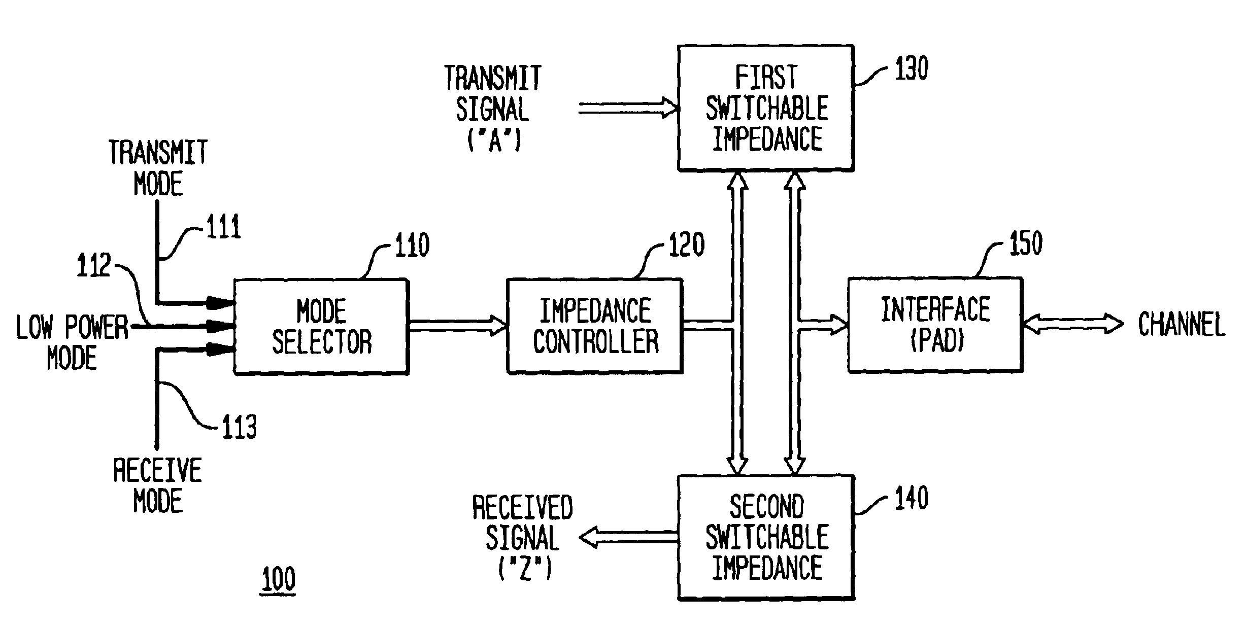
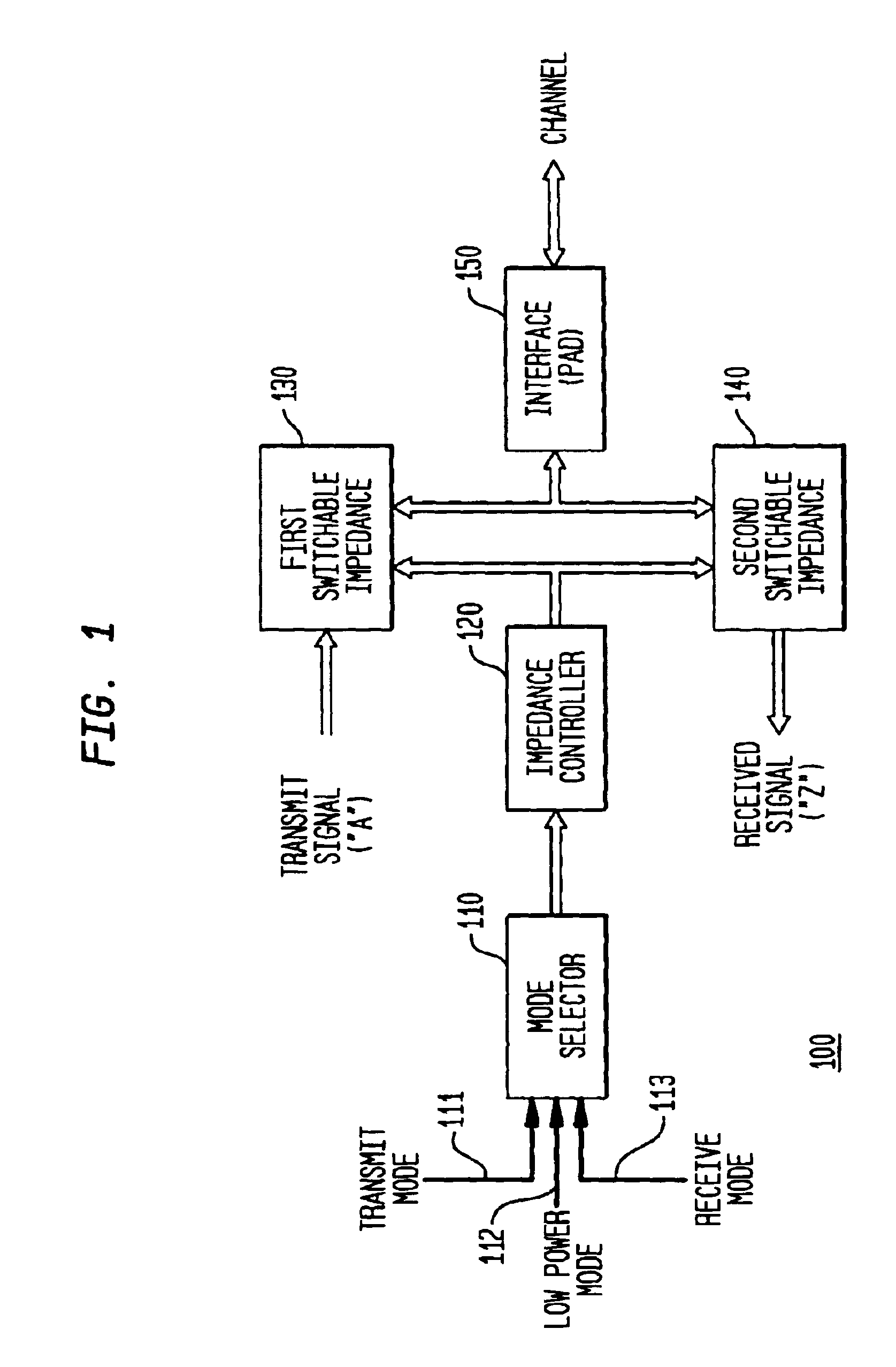
FIG. 1 (or “FIG. 1”) is a block diagram illustrating a first exemplary apparatus embodiment 100 in accordance with the present invention. As illustrated in FIG. 1, the apparatus 100 includes a mode selector 110, an impedance controller 120, a first switchable impedance 130, and a second switchable impedance 140. The apparatus 100 is generally couplable to a single interface 150 (also referred to as a “PAD” or input / output (I / O) node), which provides for an electrical interface between the apparatus 100 and the channel (transmission line or external load), for full duplex, digital communication over a channel, such as a communication bus for data transfer between and among ICs.

The apparatus 100 provides three different modes of operation: a transmit (or first) mode, a receive (or second) mode, and a low power or third mode. In the transmit mode, a signal to be transmitted (referred to herein as the “transmit signal”), consisting of digital information (or bits) referred to as “A”, wi...

embodiment 300

FIG. 2 also illustrates a third exemplary apparatus embodiment 300 in accordance with the present invention, as an abbreviated version of apparatus 200. In the event a less complicated or smaller impedance matching circuit is desired (compared to the apparatus 200), portions of the first switchable impedance 230A and 230B may be omitted, namely, transistors M9, M10, M11 and M12, and resistors 240 and 250. In these circumstances, in the transmit mode, when “A” is high, the output impedance is resistor 235 (R1), while when transmit signal “A” is low, the output impedance is R3 (resistor 245). For example, if R1 and R3 are each 100 Ohms, then the output impedance in this abbreviated circuit is 100 ohms. Conversely, for the receive mode, the input impedance is R1 in a parallel combination with R3 which, for this example, would be 50 Ohms. As a result, for this abbreviated apparatus 300, either the input impedance or the output impedance will substantially match the channel impedance; ho...

embodiment 210

In the embodiment 210, the mode selector includes an enable signal input 210; a termination enable signal input 212; a first inverter (X3) coupled to the enable signal input to provide the inverted enable signal; and a second inverter (X4) coupled to the termination enable signal input to provide the inverted termination enable signal.

In the embodiment 220, the impedance controller includes a first transmission gate 255 having an input of a signal for transmission, and is coupled to the mode selector 210 to receive the termination enable signal and the inverted termination enable signal; a NAND gate 265 having a first input 266 coupled to an output of the first transmission gate 255 and a second input 267 coupled to the mode selector to receive the enable signal; a second transmission gate 260 having an input of the signal for transmission, and coupled to the mode selector 210 to receive the termination enable signal and the inverted termination enable signal; and a NOR gate 270 hav...


PUM


Abstract

The present invention provides a bi-directional impedance matching integrated circuit which is couplable through an interface to a channel for signal transmission and reception. The invention includes a first switchable impedance and a second switchable impedance having a respective output impedance and input impedance substantially equal to a channel impedance. An impedance controller is capable of coupling the first switchable impedance to the interface in response to a transmit control signal, coupling the second switchable impedance to the interface in response to a receive control signal, and further capable of uncoupling the first switchable impedance and the second switchable impedance from a power supply and from a ground potential in response to a low power control signal. A mode selector is utilized to provide the transmit control signal, the receive control signal, and the low power control signal.

Description

FIELD OF THE INVENTIONThe present invention relates, in general, to impedance matching circuits, and, in particular, to bi-directional impedance matching integrated circuits for signal transmission and reception.BACKGROUND OF THE INVENTIONHigh speed buffers (or drivers) are used to transmit signals on a communication channel between and among integrated circuits (“ICs”). A signal to or from an IC is transmitted or received via a conductive interface material, typically referred to as a “PAD”, which provides a signaling interface and physical connection between the IC and the channel.In some cases, use of such high speed buffers often results in poor signal integrity of the transmitted signal due to an impedance mismatch between the high speed buffer output impedance (“RO”) and the channel impedance (“ZO”). In other cases, poor signal integrity of a received signal often results from an impedance mismatch between the terminating or input impedance (“RT”) (present at the PAD or other ...

Claims


Application Information

Patent Timeline
Patent Type & Authority Patents(United States)
IPC IPC(8): H04L25/02
CPCH04L25/0278H04L25/0292H04L25/028
Inventor MORRIS, BERNARD LEE
Owner AVAGO TECH INT SALES PTE LTD
Learn More