
Dual damascene bond pad structure for lowering stress and allowing circuitry under pads

a bond pad and damascene technology, applied in the field of integrated circuits, can solve the problems of leaking current through the dielectric, defect in the dielectric film over which the bond pad is typically formed, and relative large dimensions

Inactive Publication Date: 2005-01-04
BELL SEMICON LLC
View PDF15 Cites 51 Cited by
  • Summary
  • Abstract
  • Description
  • Claims
  • Application Information

AI Technical Summary

Problems solved by technology

Due to conventional bonding technology used to couple external conductive wires to the bond pads, and also due to design constraints, the bond pads have relatively large dimensions when compared to other features such as transistors or other individual devices which combine to form the integrated circuit device.
These conditions used for coupling the wire to the bond pad, however, can cause defects in a dielectric film over which the bond pad is typically formed.
The stresses may cause defects which can result in leakage currents through the dielectric formed between the bond pads and the underlying substrate, which is frequently electrically conducting, and other devices if they are formed beneath the bond pads.
As such, using conventional processing technology, these leakage currents preclude incorporating active devices beneath the bond pads.
This limitation decreases the level of integration and the efficient use of substrate space for device purposes.
These additional processing steps take time and add production and material costs to the production of an integrated circuit.

Method used


Image

  • Dual damascene bond pad structure for lowering stress and allowing circuitry under pads
  • Dual damascene bond pad structure for lowering stress and allowing circuitry under pads
  • Dual damascene bond pad structure for lowering stress and allowing circuitry under pads

Examples


Embodiment Construction

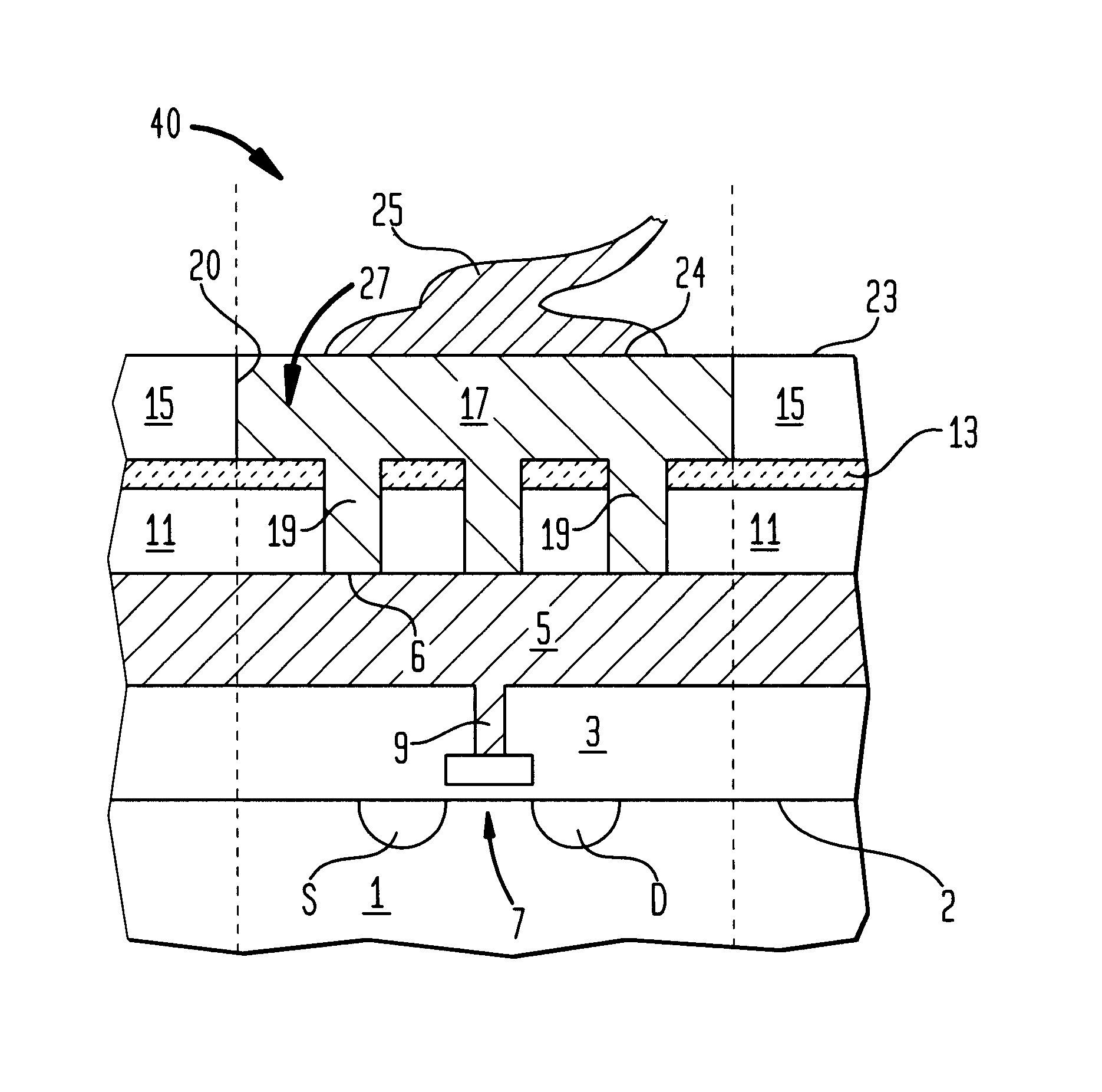
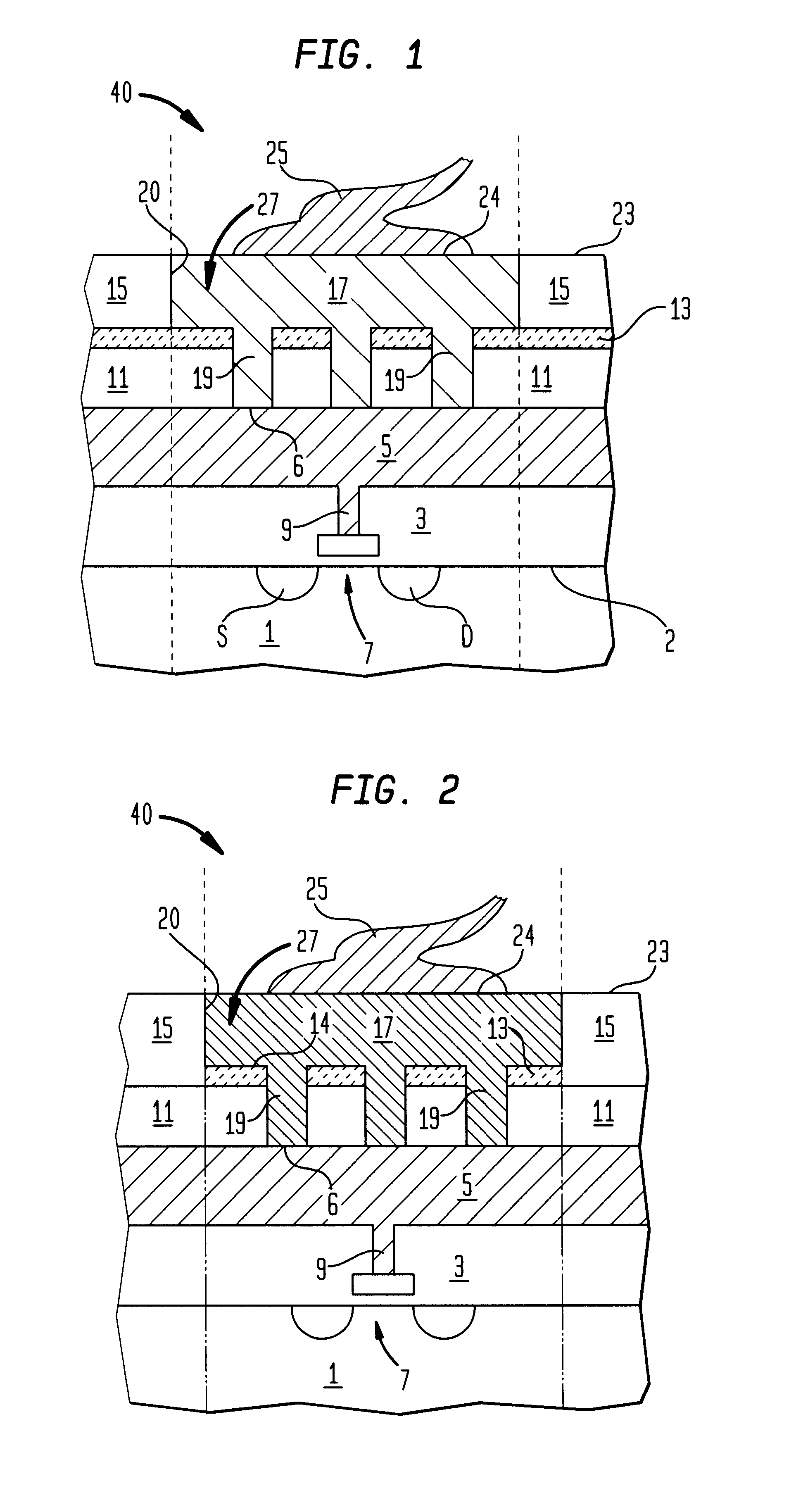
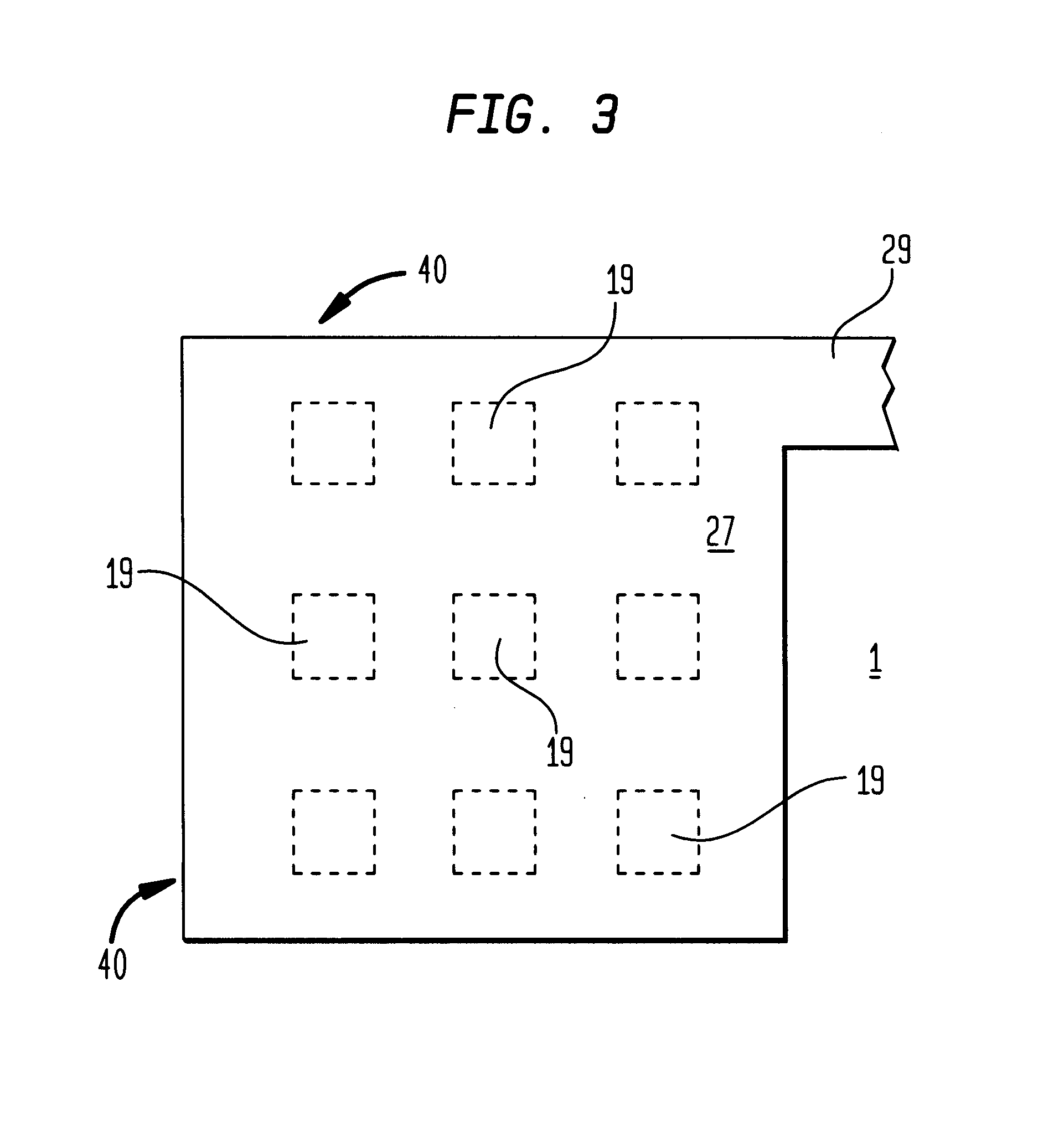
FIG. 1 is a cross-sectional view showing the bond pad structure of the present invention. Bond pad 27 is formed within bond pad region 40 formed over substrate 1. Within bond pad region 40 and beneath bond pad 27, active devices such as transistor 7 may be formed.

More particularly, FIG. 1 shows bond pad 27 formed within bond pad region 40 over substrate 1. Substrate 1 may be any suitable substrate on which semiconductor devices and integrated circuits are formed. In an exemplary embodiment, substrate 1 may be a silicon wafer. Bond pad 27 is formed of metal film 17. Metal film 17 may be any suitable metal film used as a conductive film within an integrated circuit. Examples of such conductive films include tungsten, aluminum, copper and their alloys such as AlCuSi. In other exemplary embodiments (not shown), metal film 17 may be a composite film including one of the metal films described above, and another film such as a barrier layer film.

Bond pad 27 includes lower surface 14 which ...


PUM


Abstract

A bond pad is located over active circuitry formed within an integrated circuit device. A barrier film forms the bottom surface of the upper portion of a bond pad opening which also includes vias extending through the bottom surface to form a dual damascene structure. The bond pad is resistant to stress effects such as cracking, which can be produced when bonding an external wire to the bond pad, and therefore prevents leakage currents between the bond pads and the underlying circuitry.

Description

FIELD OF THE INVENTIONThis invention relates generally to the field of integrated circuits and particularly to such integrated circuits having at least a portion of the active circuitry positioned under the bond pads.BACKGROUND OF THE INVENTIONAs today's advancing semiconductor processing technology allows for higher integration levels within integrated circuit devices, it becomes increasingly more important to fully utilize the space available within the substrates on which the integrated circuit devices are produced. An integrated circuit device is also known as a chip especially when it is still included within the semiconductor substrate on which it is formed. Chip size is determined, in large part, by the density and number of individual devices which combine to form a completed integrated circuit device. By minimizing or reducing chip size, more chips can be created within a substrate of a fixed dimension, and production costs are therefore decreased.Each integrated circuit de...

Claims


Application Information

Patent Timeline
IPC IPC(8): H01L21/60H01L23/48H01L21/70H01L23/485H01L21/02H01L23/532H01L21/768H01L23/52
CPCH01L21/76807H01L24/05H01L24/11H01L24/48H01L23/53209H01L2224/05556H01L2224/04042H01L2224/05093H01L2224/05096H01L2224/05166H01L2224/05187H01L2224/05546H01L2224/05624H01L2224/05647H01L2224/05684H01L2224/13099H01L2224/48463H01L2224/85399H01L2924/01005H01L2924/01006H01L2924/01013H01L2924/01014H01L2924/01022H01L2924/01029H01L2924/0105H01L2924/01073H01L2924/01074H01L2924/01082H01L2924/04941H01L2924/04953H01L2924/14H01L2224/05554H01L2224/0401H01L2924/10253H01L2924/01033H01L2924/00014H01L2224/45099H01L2924/00H01L21/76813
Inventor CHITTIPEDDI, SAILESHCOCHRAN, WILLIAM THOMASSMOOHA, YEHUDA
Owner BELL SEMICON LLC
Learn More