Method for forming a double-gated semiconductor device
a semiconductor device and double-gate technology, applied in the field of semiconductor devices, can solve the problems of reducing the mobility of carriers and junction characteristics, not demonstrating short-channel effects such as leakage and threshold voltage stability, and unable to maintain high drive curren
- Summary
- Abstract
- Description
- Claims
- Application Information
AI Technical Summary
Problems solved by technology
Method used
Image

Examples
Embodiment Construction
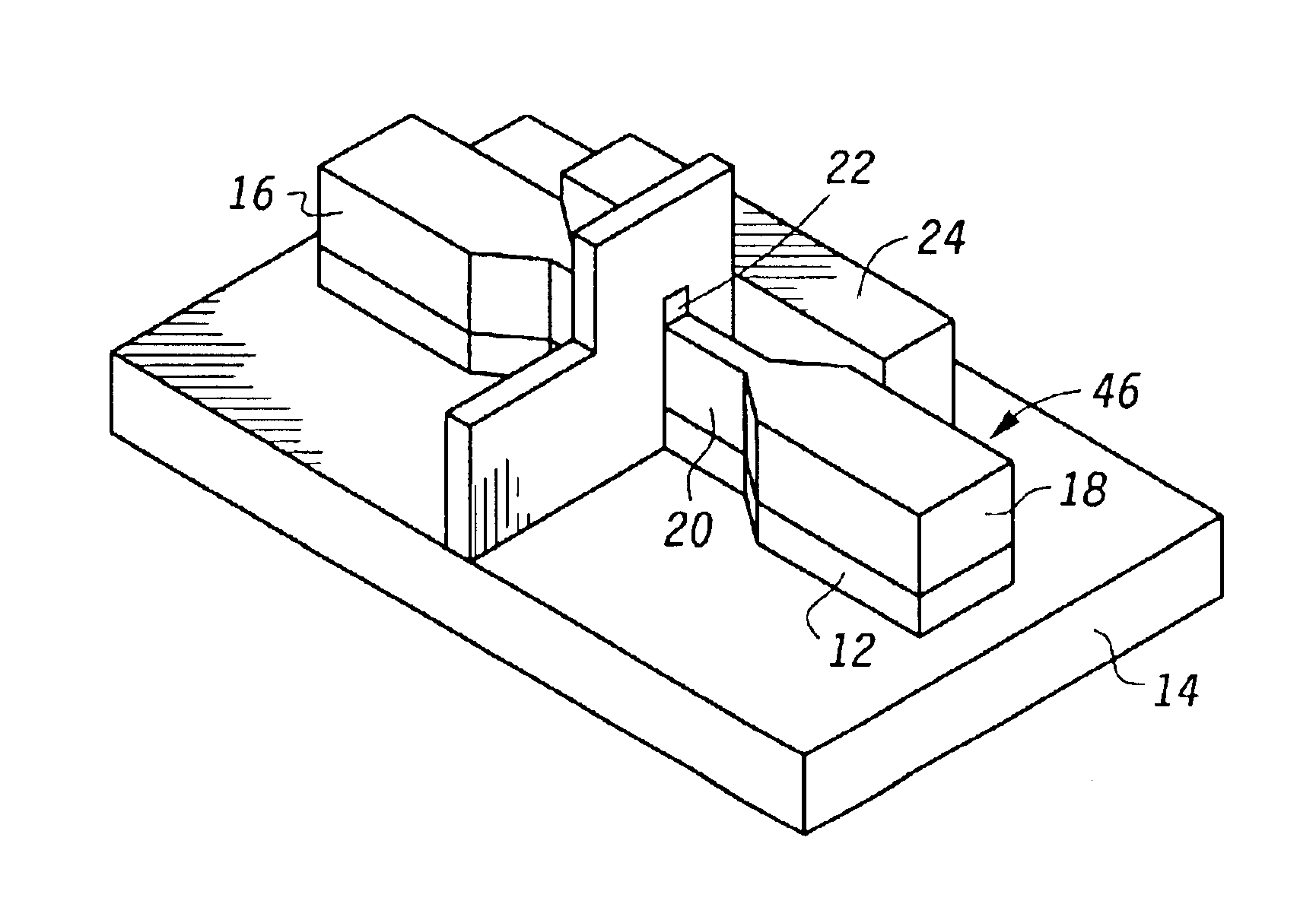
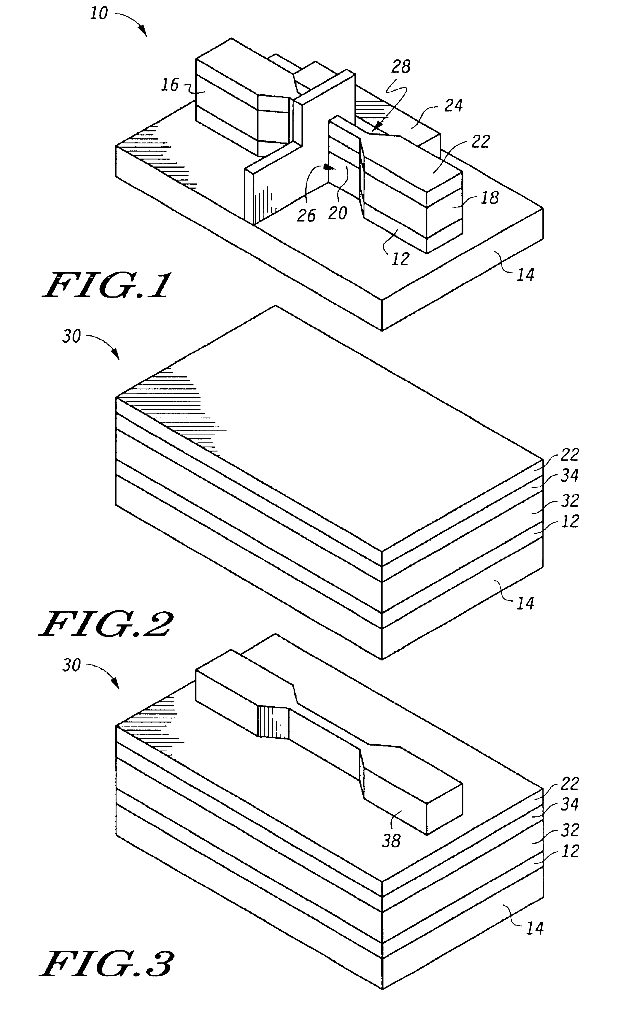
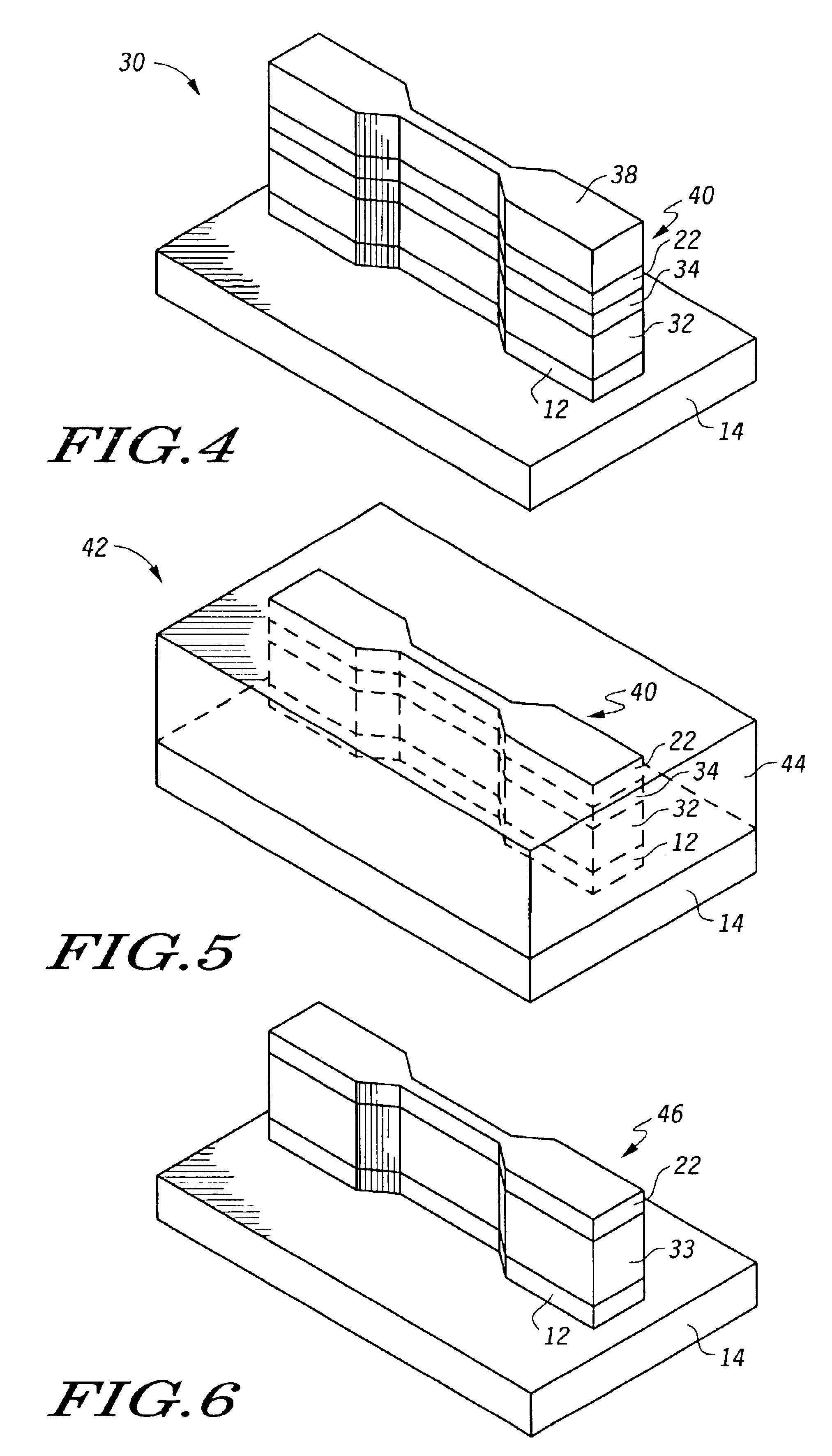
Generally, the present invention provides a method for forming a double-gated semiconductor device using a polysilicon film that exhibits a sufficiently large grain size to form a FinFET or similar device having desirable operational characteristics. FIG. 1 shows a perspective view of one embodiment of the present invention as a vertical, self-aligned double-gated polysilicon FinFET 10 built including an insulative layer 12 over silicon substrate 14. Between source 16 and drain 18, polysilicon FinFET 10 includes channel 20. Dielectric layer and hard mask 22 covers source 16, drain 18, and channel 20. Source 16, drain 18, and channel 20 are formed through a process that begins with the deposition of an amorphous silicon layer.
As the discussion which follows explains in greater detail, the process of the present invention anneals the amorphous silicon layer to yield a polysilicon layer. Source 16, drain 18, and channel 20 are defined by patterning and etching the polysilicon layer. A ...
PUM
 Abstract
Description
Claims
Application Information
 - R&D
- Intellectual Property
- Life Sciences
- Materials
- Tech Scout
- Unparalleled Data Quality
- Higher Quality Content
- 60% Fewer Hallucinations
Browse by: Latest US Patents, China's latest patents, Technical Efficacy Thesaurus, Application Domain, Technology Topic, Popular Technical Reports.
© 2025 PatSnap. All rights reserved.Legal|Privacy policy|Modern Slavery Act Transparency Statement|Sitemap|About US| Contact US: help@patsnap.com