
Bandgap voltage reference circuit and method for producing a temperature curvature corrected voltage reference

Inactive Publication Date: 2004-12-07
ANALOG DEVICES INC
View PDF13 Cites 64 Cited by
  • Summary
  • Abstract
  • Description
  • Claims
  • Application Information

AI Technical Summary

Benefits of technology

The advantages of the invention are many. The bandgap voltage reference provides a temperature stable voltage reference which is corrected for TlnT temperature curvature, and the voltage reference is stable over a relatively wide temperature range, and in particular over the temperature range of -40.degree. C. to +120.degree. C. Indeed, it is believed that the voltage reference is temperature stable over an even wider temperature range. Furthermore, the bandgap voltage reference circuit according to the invention is a relatively non-complex circuit, and can be readily easily implemented in a CMOS process with a relatively low die area requirement. This advantage has been achieved by virtue of the fact that the circuit can be constructed with the collectors of the first and second transistors tied to the same voltage level, which can be ground or any other suitable common voltage level. The PTAT voltage generated by the bandgap voltage reference circuit according to the invention as well as having a positive temperature coefficient, also has a curvature of TlnT form which is complementary to the TlnT curvature of a CTAT base-emitter voltage of a transistor, and thus, the PTAT voltage developed by the bandgap voltage reference circuit is ideally suited to correcting for the TlnT temperature curvature of the negative temperature coefficient of the base-emitter CTAT voltage of a transistor for producing a temperature stable TlnT temperature curvature corrected reference voltage. The fact that the CTAT correcting current is derived from the base-emitter CTAT voltage of one of the first transistors leads to the simplicity and temperature stability of the circuit.
In particular, the simplicity of the circuit according to the invention is achieved by virtue of the fact that the correcting PTAT voltage with the TlnT temperature curvature correction voltage are developed simultaneously across one single resistor, namely, the primary resistor in the bandgap cell. This leads to considerable simplification of the bandgap circuit, and furthermore, minimises the sensitivity of the bandgap circuit to process variations.

Problems solved by technology

However, while the voltage reference developed by the bandgap circuit of Audy is TlnT curvature corrected, and is thus temperature stable within a relatively wide temperature range, unfortunately, the bandgap circuit of Audy does not lend itself to easy implementation in a CMOS process.
However, the circuitry required for implementing the bandgap voltage reference circuit of Nguyen is relatively complex, and additionally, it does not lend itself to a CMOS process.
The circuitry of the Rincon-Mora bandgap voltage reference circuit is relatively complex, and does not easily lend itself to implementation in a CMOS process.
However, the TlnT temperature curvature compensation of the bandgap voltage reference circuit of Sundby is not particularly accurate, and use of resistors with high temperature coefficients is not desirable.
However, since the compensating circuit varies the current flowing through the compensating resistor in steps in response to predetermined temperature threshold values, the temperature curvature correction provided by this circuit is relatively inaccurate, and furthermore, the circuit is a relatively complex circuit.
However, the temperature curvature correction provided by the curvature correction circuit is of limited accuracy and does not adequately compensate for TlnT curvature.
Furthermore, the circuit of Carvajal does not lend itself easily to implementation by a CMOS process.
However, the circuitry of Nelson is relatively complex, and does not lend itself to easy implementation in a CMOS process.
The temperature stability of the voltage reference of this circuit is limited, since the curvature correction is reliant solely on non-linear resistors.
This circuit of Lewis does not easily lend itself to implementation in a CMOS process, and additionally, TlnT temperature curvature correction is limited.

Method used


Image

  • Bandgap voltage reference circuit and method for producing a temperature curvature corrected voltage reference
  • Bandgap voltage reference circuit and method for producing a temperature curvature corrected voltage reference
  • Bandgap voltage reference circuit and method for producing a temperature curvature corrected voltage reference

Examples


Embodiment Construction

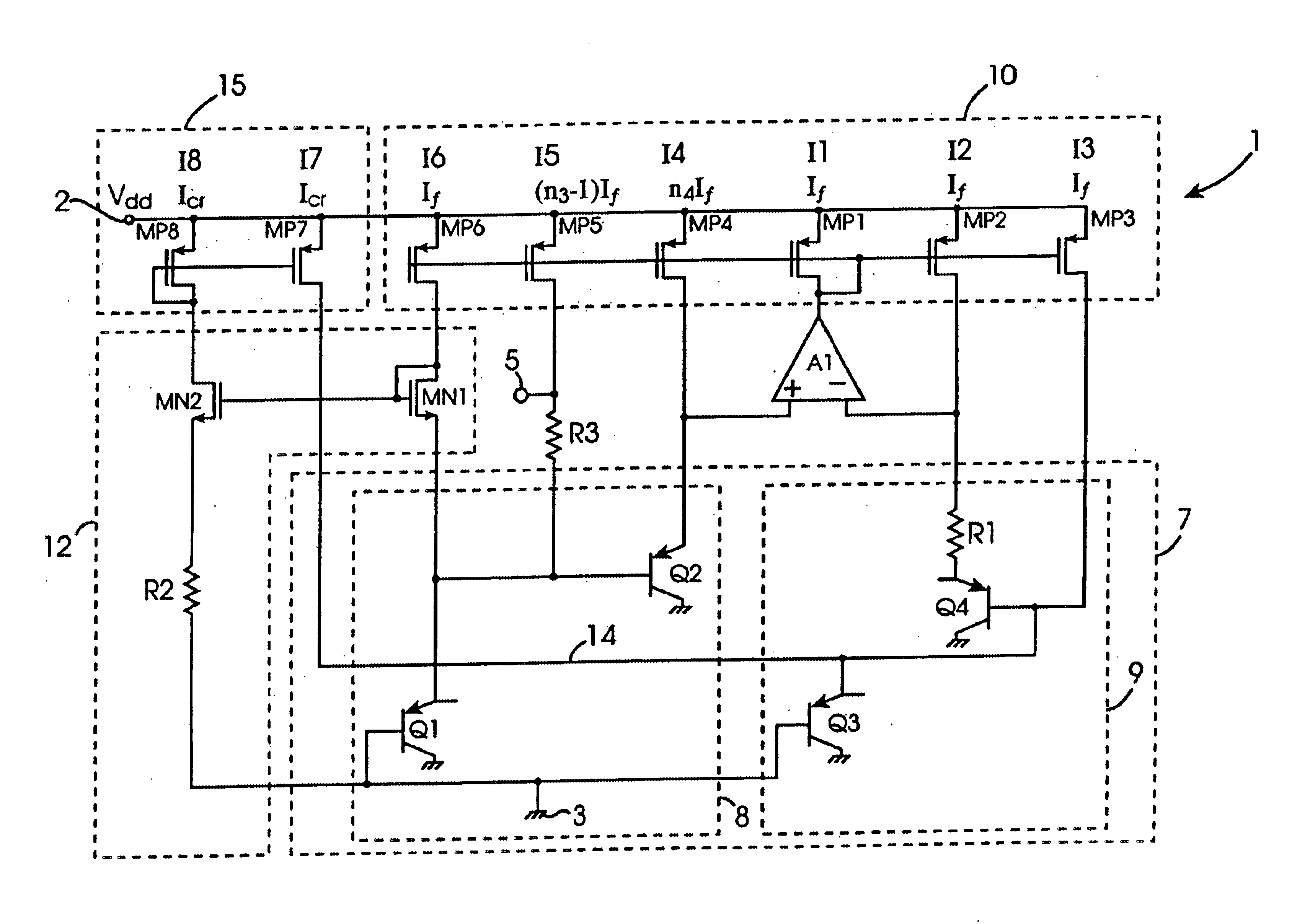
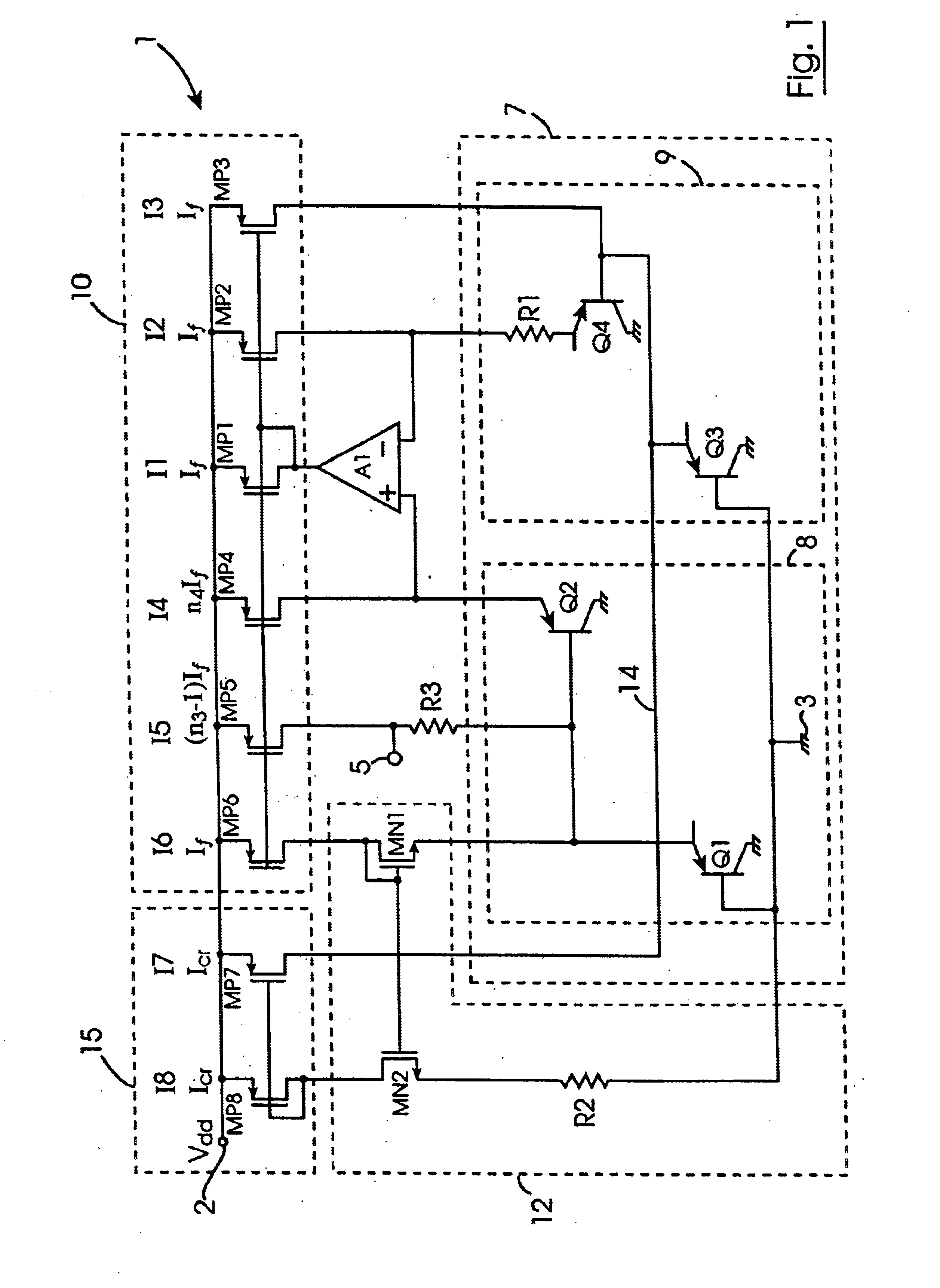
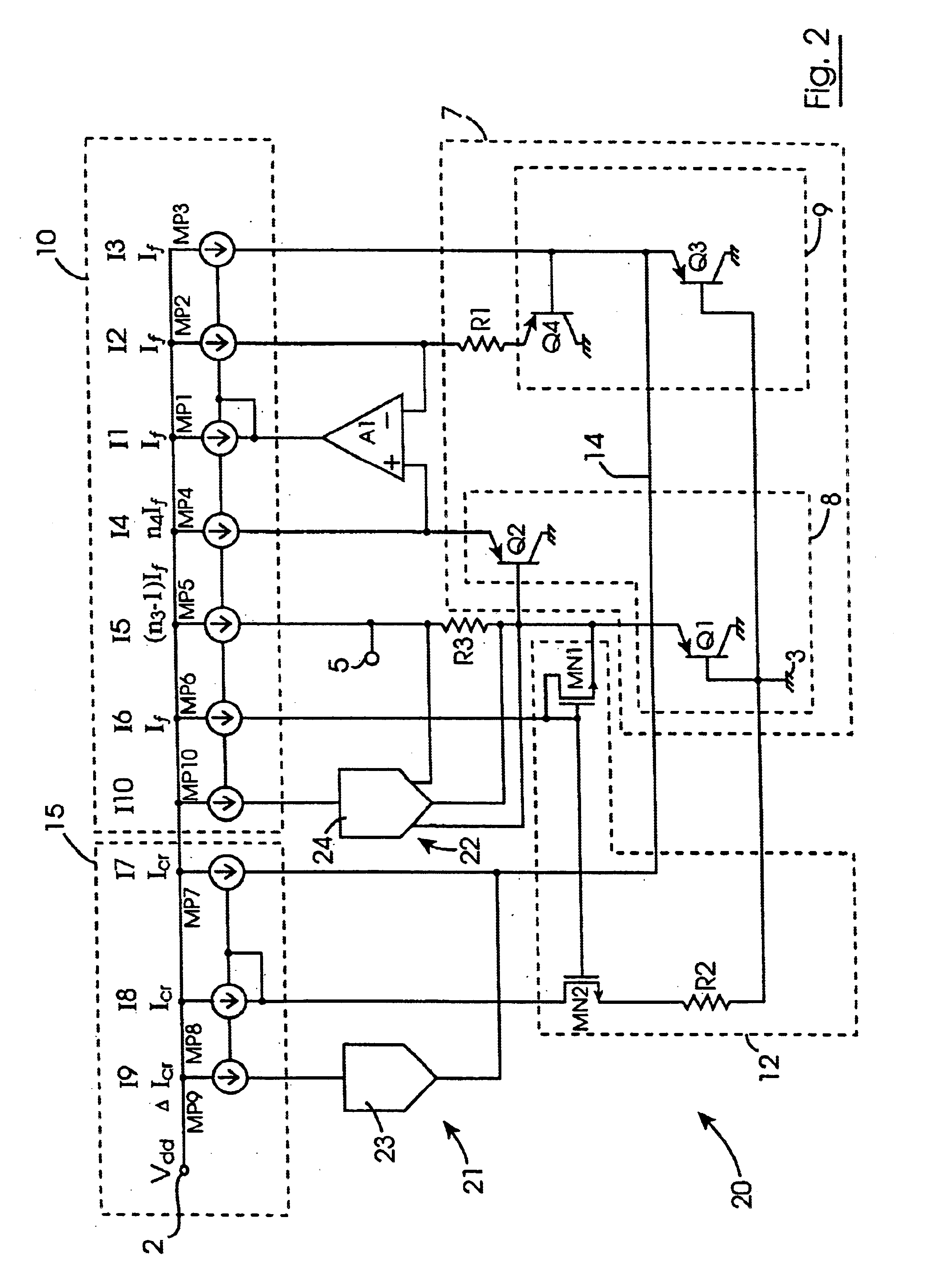
Referring to the drawings and initially to FIG. 1 there is illustrated a bandgap voltage reference circuit according to the invention indicated generally by the reference numeral 1 for providing a temperature stable DC voltage reference output with TlnT temperature curvature correction. The voltage reference circuit 1 is implemented as an integrated circuit on a silicon chip by a CMOS process. The voltage reference circuit 1 is supplied with a supply voltage V.sub.dd on a supply rail 2, and the voltage reference circuit 1 is grounded at 3. The temperature stable TlnT temperature curvature corrected voltage reference is developed between an output terminal 5 and ground 3.

The voltage reference circuit 1 comprises a bandgap cell 7, which comprises a first transistor stack 8 comprising two stacked transistors, namely, two first bipolar transistors Q1 and Q2, and a second transistor stack 9 comprising two stacked transistors, namely, two second bipolar transistors Q3 and Q4. The first an...


PUM


Abstract

A bandgap voltage reference circuit (1) comprises a bandgap cell (7) comprising first and second transistor stacks (8,9) of first transistors (Q1,Q2) and second transistors (Q3,Q4), respectively, arranged for developing a correcting PTAT voltage (DeltaVbe) across a primary resistor (R1) proportional to the difference in the base-emitter voltages of the first and second transistor stacks (8,9). A first current mirror circuit (10) provides PTAT currents (12 to 15) to the emitters of the first and second transistors (Q1 to Q4), and an operational amplifier (A1) maintains the voltage on the emitter of the first transistor (Q2) of the first transistor stack (8) at the same level as the resistor (R1) and sinks a PTAT current from the first current mirror circuit (10) from which the other PTAT currents are mirrored. The correcting PTAT voltage (DeltaVbe) developed across the primary resistor (R1) is scaled onto a secondary resistor (R3) and summed with the uncorrected base-emitter CTAT voltage of the first transistor (Q1) of the first transistor stack (8) for providing the voltage reference between an output terminal (5) and ground (3). A CTAT correcting current (Icr) is summed with the PTAT current (13) and applied to the emitter of the second transistor (Q3) of the second transistor stack (9) so that the correcting PTAT voltage (DeltaVbe) developed across the primary resistor (R1) has a TlnT curvature complementary to the TlnT temperature curvature of the uncorrected base-emitter CTAT voltage of the first transistor (Q1). Thus the reference voltage developed between the output terminal (5) and the ground (3) is temperature stable and TlnT temperature curvature corrected. The CTAT correcting current is derived from the base-emitter CTAT voltage of the first transistor (Q1) in a CTAT current generating circuit (12) through a second current mirror circuit (15).

Description

The present invention relates to a bandgap voltage reference circuit for producing a stable TlnT temperature curvature corrected voltage reference, which preferably is suitable for fabrication in a CMOS process, and the invention also relates to a PTAT voltage generating circuit for generating a PTAT voltage with a temperature curvature complementary to an uncorrected TlnT temperature curvature CTAT voltage of the type developed across a base-emitter of a transistor, which preferably is suitable for fabrication in a CMOS process. The invention also relates to a method for producing such a voltage reference and a PTAT voltage.BACKGROUND TO THE INVENTIONMost electronic circuits require a stable DC voltage reference, and in particular, a temperature stable DC voltage reference. Bandgap voltage reference circuits for producing a reasonably temperature stable DC voltage reference are known. Such bandgap voltage reference circuits rely on the property of a bipolar transistor to produce a ...

Claims


Application Information

Patent Timeline
IPC IPC(8): G05F3/08G05F3/30
CPCG05F3/30
Inventor MARINCA, STEFAN
Owner ANALOG DEVICES INC
Learn More