
Plasma chamber conditioning

a technology of plasma chamber and conditioning chamber, which is applied in the direction of electrical equipment, basic electric elements, electric discharge tubes, etc., can solve the problems of particle on the wafer surface, affecting yield, and yield loss

Inactive Publication Date: 2003-12-02
LAM RES CORP
View PDF5 Cites 131 Cited by
  • Summary
  • Abstract
  • Description
  • Claims
  • Application Information

AI Technical Summary

Benefits of technology

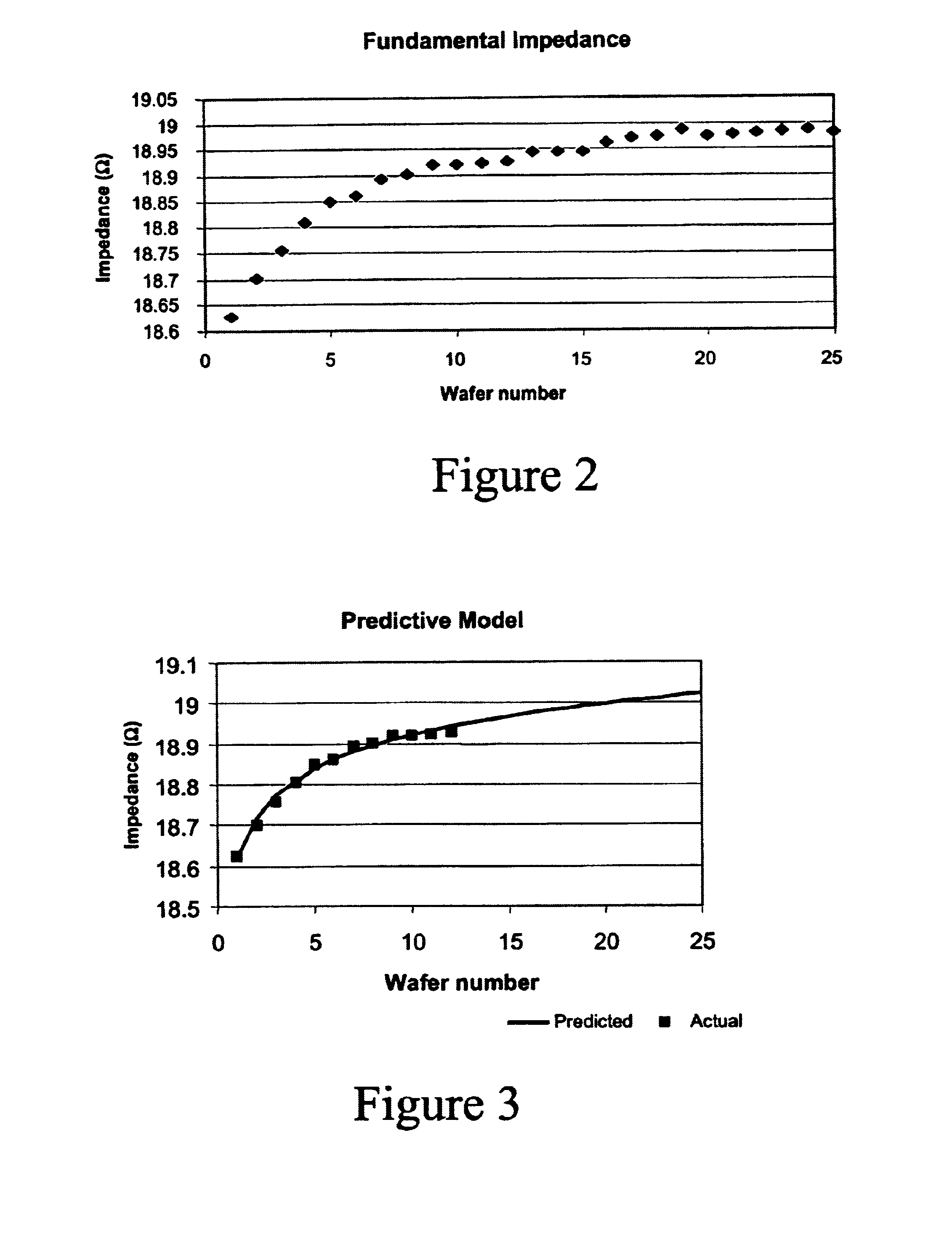
This invention provides several advantages over the existing known methods. Firstly, the number of conditioning wafers may be optimised so that the amount of downtime is minimised. Secondly, the number of qualification wafers is reduced as these wafers are loaded only when the predictive model indicates that the chamber will reach equilibrium.

Problems solved by technology

If this material were not periodically removed, it would eventually flake, depositing particles onto the wafer surface, and impacting yield.
If the chamber is not conditioned in this way, the first number of production wafers experience significantly different process conditions, resulting in yield loss.
The operator of the chamber does not know exactly how many conditioning wafers are needed to restore process conditions.
This is not an optimal method, since equilibrium conditions are often unpredictable, being a function of wafer grade, chamber configuration or the time the chamber has been exposed to atmosphere.
The conditioning step of the preventive maintenance activity can constitute a large percentage of the total preventive-maintenance downtime, thus incurring a significant cost.
This results in the generation of harmonics of the RF driving signal.
One limitation of this approach is that the operator of the chamber has no advance warning of when this event may occur, and cannot decide to continue conditioning the chamber, load qualification wafers or load production wafers into the tool.

Method used


Image

  • Plasma chamber conditioning
  • Plasma chamber conditioning
  • Plasma chamber conditioning

Examples


Embodiment Construction

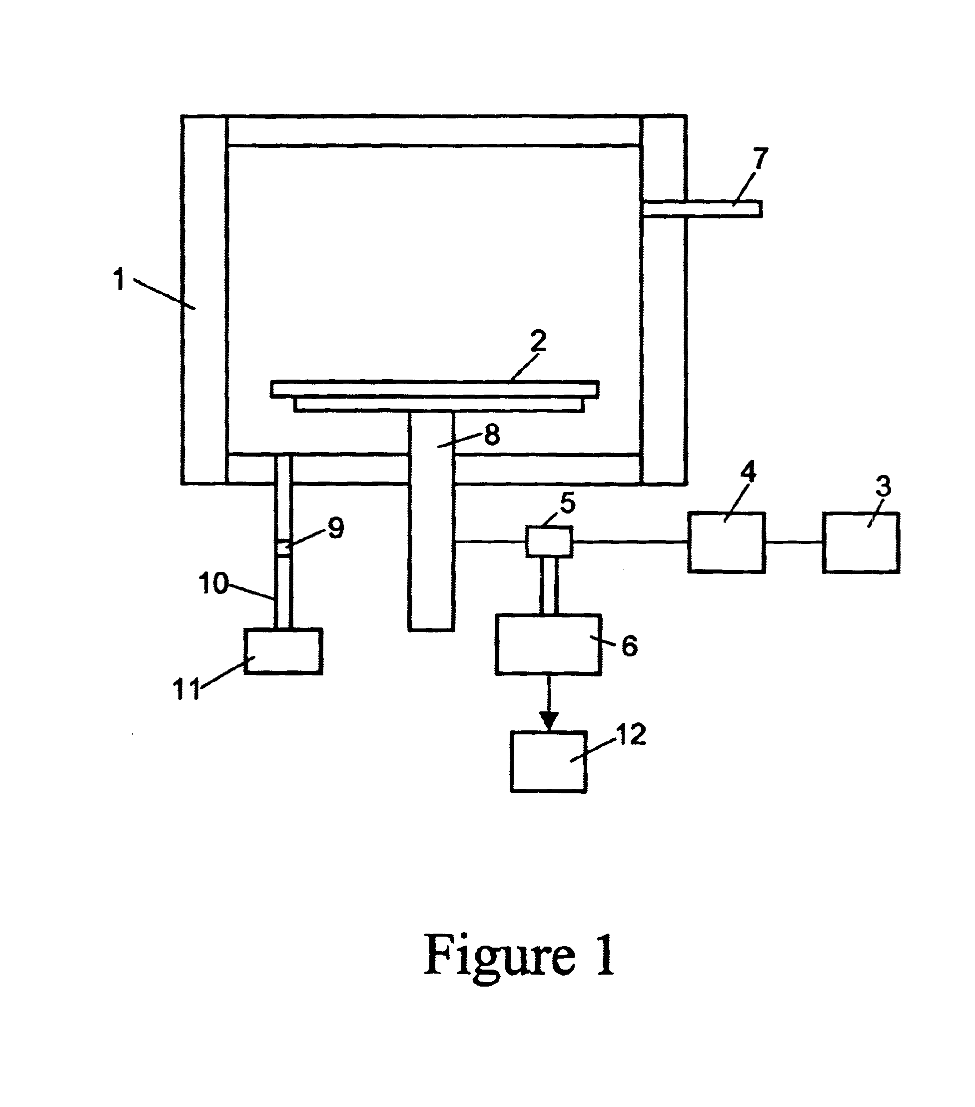
FIG. 1 shows a typical plasma process reactor. It includes a plasma chamber 1 containing a wafer or substrate 2 to be processed. A plasma is established and maintained within the chamber by an RF power source 3. This source generally has real impedance which must undergo a transformation to match that of the complex plasma load. This is done via match network 4. Power is coupled to the plasma chamber, typically by capacitive coupling, through an electrode 8. However, the invention also applies to systems that have more than one capacitive electrode, those that are inductively coupled or transformer coupled, helical / helicon wave systems and electron-cyclotron resonance systems. Process gases are admitted through gas inlet 7 and the chamber is maintained at a desired process pressure by removing process gases and by-products through gas exhaust line 10 using pump 11. A throttle valve 9 may be used to control process pressure in an automatic control loop.

The wafer is processed accordin...


PUM


Abstract

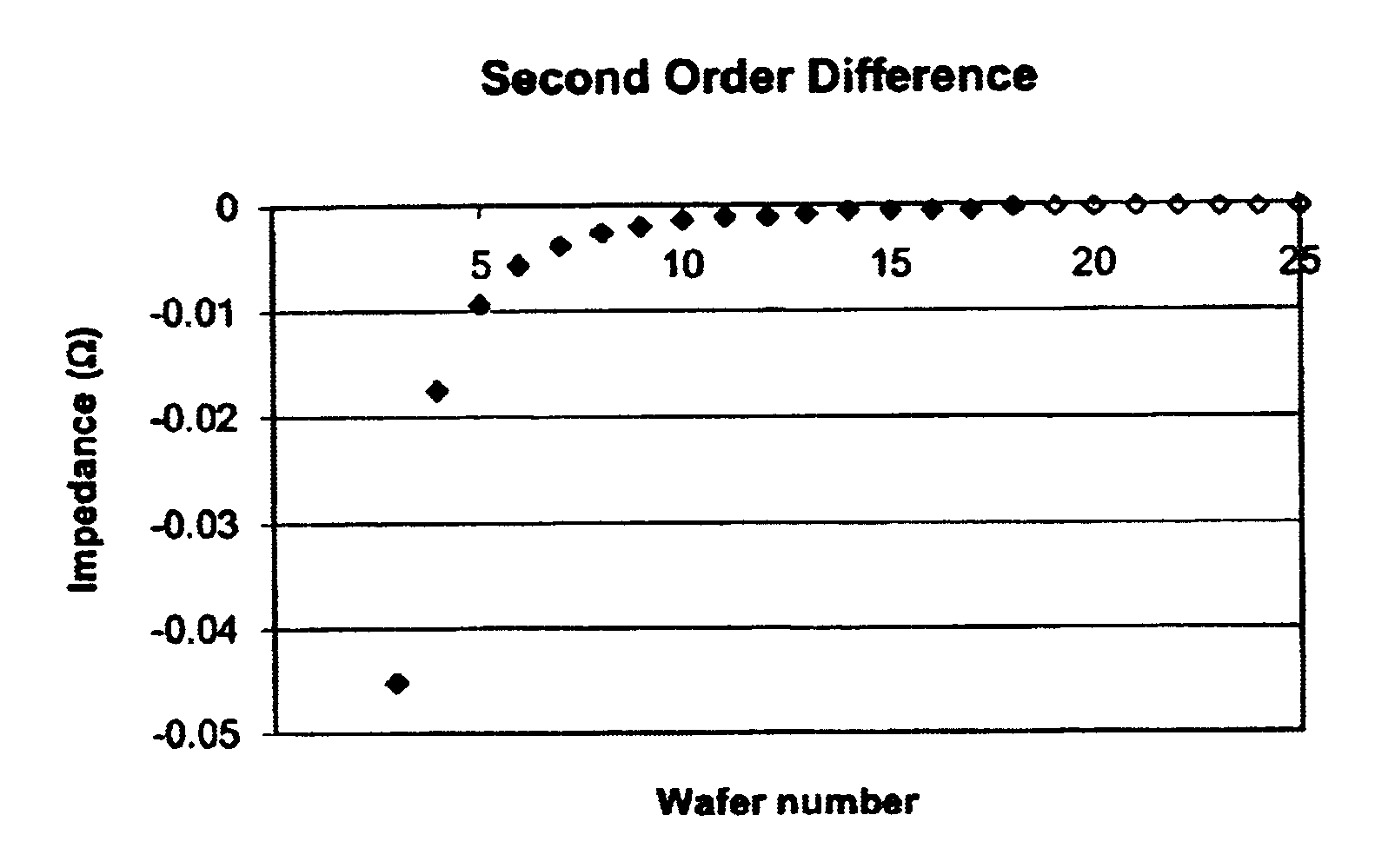
A method for determining the optimum number of conditioning wafers to be run following a wet clean of the walls of an RF plasma chamber 1 is based on an electrical precursor signal. Polymer build up on a plasma chamber wall during normal chamber conditioning is monitored by observing components of the fundamental RF signal. After a pre-determined number of wafers has been run, a predictive model is used to determine the total number of wafers needed to complete the conditioning cycle.

Description

1. Field of the InventionThe present invention relates to a method of conditioning an RF-powered plasma processing chamber after cleaning the interior chamber walls.2. Prior ArtMany thin film processes use plasma processes to facilitate the rapid and accurate fabrication of minute structures with desired properties. Plasma processes include the deposition and etching of insulators, conductors and semiconductors on a substrate, for example, a silicon wafer. The plasma process usually involves placing the substrate in a vacuum chamber, introducing process gases and applying radio-frequency (RF) power, typically 0.1 to 200 MHz, to create a plasma. The plasma consists of ions, electrons, radical gas species and neutral gas, all of which permit the desired reaction to proceed. The plasma reaction has many inputs, including RF power, gas type and flow rates, chamber pressure, substrate and wall temperatures, chamber wall conditions, electrode spacing, and so on.The chamber configuration a...

Claims


Application Information

Patent Timeline
IPC IPC(8): H01J37/32H01L21/00
CPCH01J37/32009H01J37/32862H01L21/67253H01L21/67069
Inventor SCANLAN, JOHNO'LEARY, KEVINCOONAN, BARRY
Owner LAM RES CORP
Learn More