Adjustment of the partial coherence of the light energy in an imaging system

a technology of partial coherence and imaging system, which is applied in the direction of photomechanical equipment, instruments, printing, etc., can solve the problems of increasing the portion of the overall cd error budget consumed by within-field cd variability, increasing the proportion and increasing the cd error budget of the overall cd error budg

Inactive Publication Date: 2003-08-26
INTEL CORP
View PDF6 Cites 6 Cited by
  • Summary
  • Abstract
  • Description
  • Claims
  • Application Information

AI Technical Summary

Problems solved by technology

However, aberrations in the optics of the imaging tool have become an increasingly important determinant of gate CD variability as dimensions in the transistors shrink below 130 nanometers.
However, CD variability along the slit direction may be caused by aberrations in the optics or by non-uniform distribution of dose or partial coherence.
As gate CD on a microprocessor continually shrinks, the within-field CD variability consumes an increasingly larger portion of the overall CD error budget.
Unfortunately, a tool-specific array 110 incurs significant cost and requires a long time to build.

Method used


Image

  • Adjustment of the partial coherence of the light energy in an imaging system
  • Adjustment of the partial coherence of the light energy in an imaging system
  • Adjustment of the partial coherence of the light energy in an imaging system

Examples


first embodiment

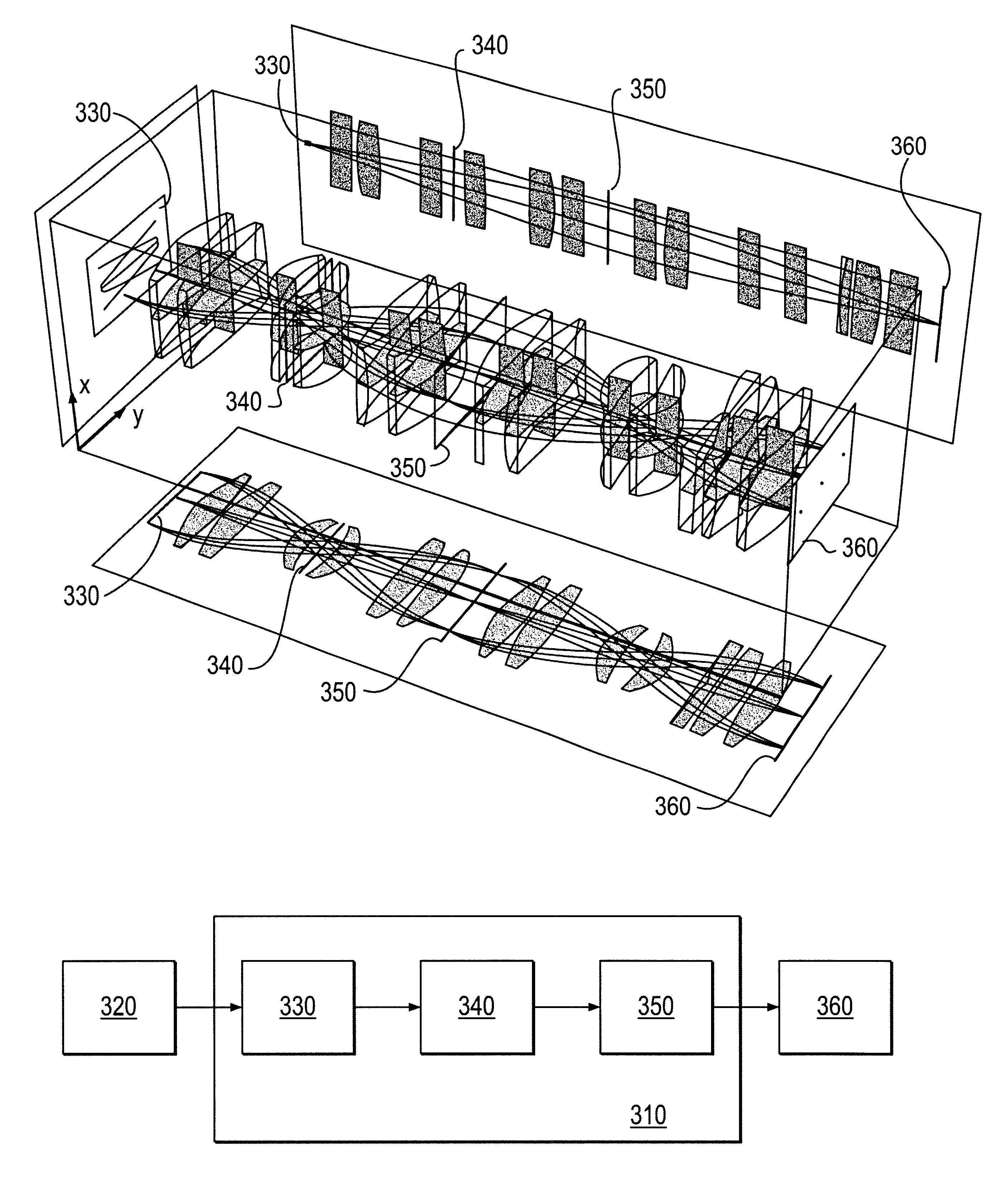
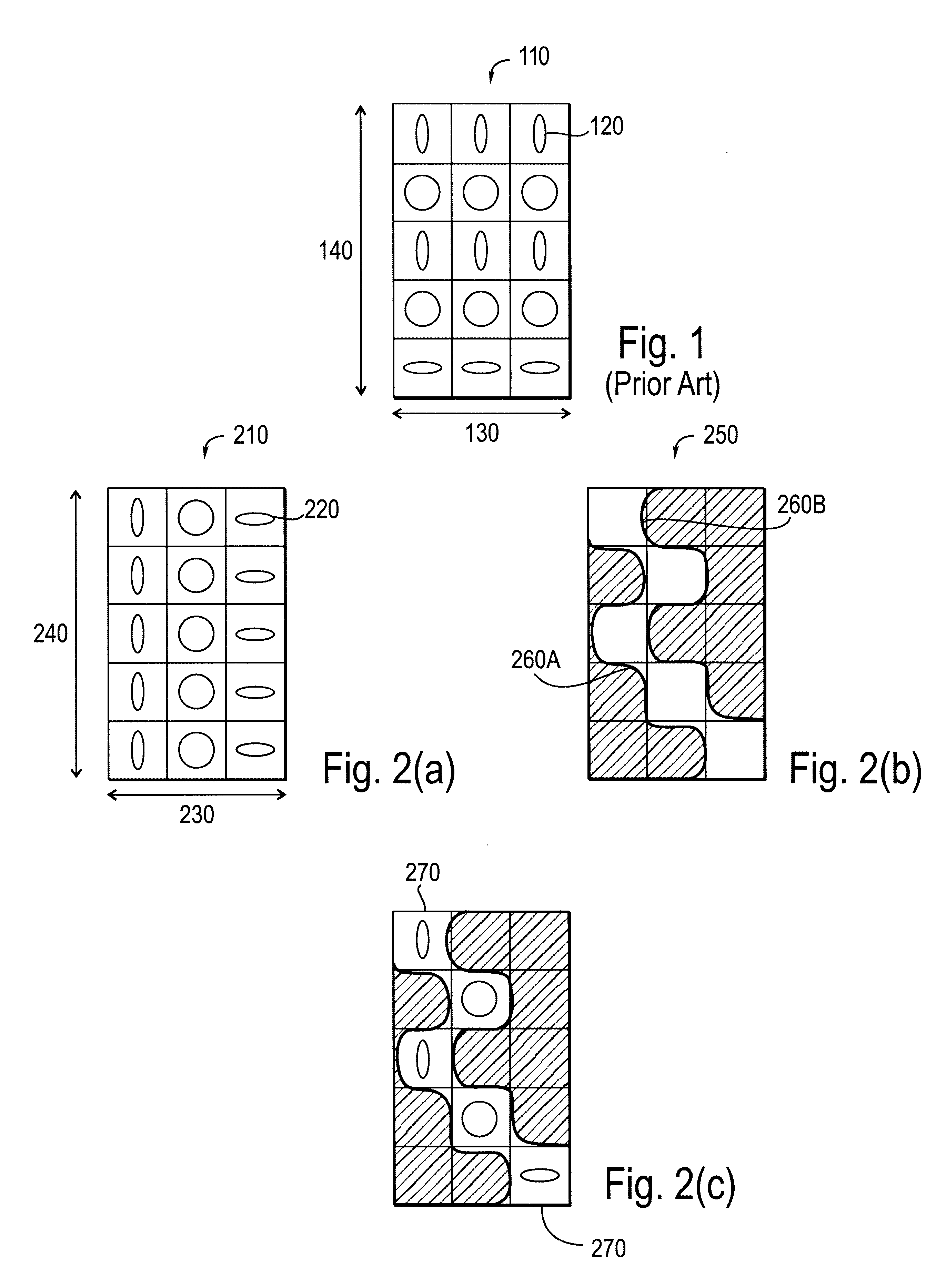
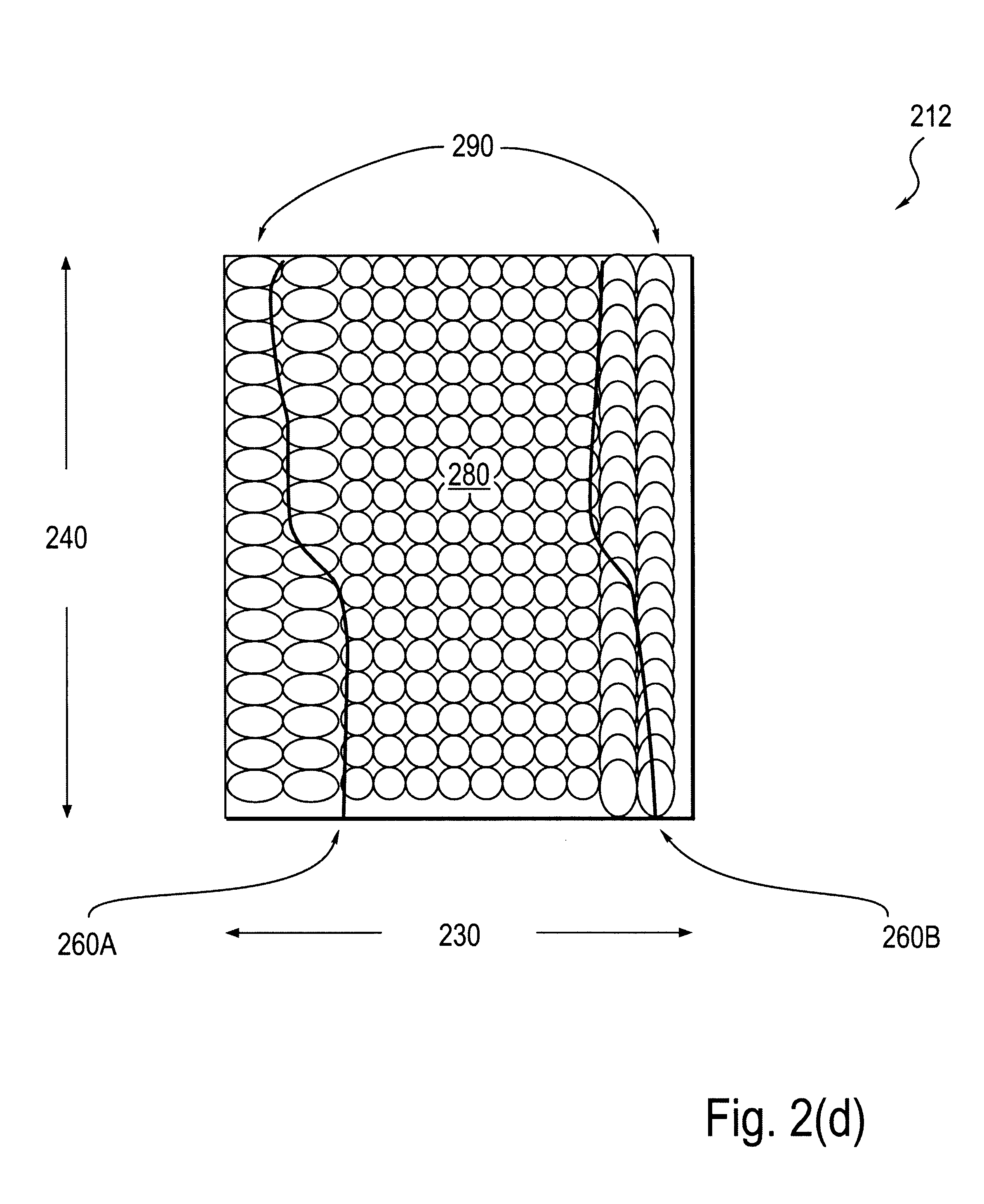
In the present invention, horizontal-vertical (H-V) bias along the direction of a slit is reduced by using an array 210, as shown in FIG. 2(a), in conjunction with an aperture 250 with articulated edges 260A and 260B, as shown in FIG. 2(b). H-V bias refers to CD variability between two orthogonal directions, in particular, the horizontal direction and the vertical direction. H-V bias varies as a function of pitch. Pitch is the periodicity in a pattern of regularly-repeating features. H-V bias may be caused by aberrations in the projection optics or non-uniformity in partial coherence of the illumination. One kind of optical aberration is astigmatism, which causes H-V bias that is very sensitive to focus. Another kind of optical aberration is coma, which causes H-V bias that is not appreciably sensitive to focus.

The array 210 is substantially planar with a first dimension 230 and a second dimension 240 that are orthogonal to each other. When a step-and-scan type of imaging tool is us...


PUM

PropertyMeasurementUnit
optical aberrationsaaaaaaaaaa
light energyaaaaaaaaaa
channel lengthsaaaaaaaaaa

Abstract

The present invention describes an apparatus comprising an optical array generating a distribution of partial coherence of light energy and an aperture to select a subset of said distribution of partial coherence.

Description

1. Field of the InventionThe present invention relates to the field of semiconductor integrated circuit (IC) manufacturing, and more specifically, to an apparatus for and a method of adjusting the partial coherence of the light energy in an imaging system, such as a step-and-scan tool used in photolithography.2. Discussion of Related ArtThe performance of a microprocessor comprising transistors is primarily determined by the channel lengths of the transistors. The channel lengths are highly dependent on the widths of the gates in the transistors. Photolithography is the process by which a pattern of gates can be transferred from a reticle to a layer of photoresist on a wafer during the fabrication of a microprocessor. The reticle is a photomask which has a pattern of gates extracted from a layout of a microprocessor. Photoresist is a radiation-sensitive material. Radiation is the transfer of energy as waves or particles. The application of radiation in the form of light, electron, o...

Claims


Application Information

Patent Timeline
Patent Type & Authority Patents(United States)
IPC IPC(8): G02B27/00G03F7/20
CPCB82Y10/00G02B27/0068G03F7/70075G03F7/70091G03F7/70166
Inventor GOLDSTEIN, MICHAELURATA, JOHN M.
Owner INTEL CORP
Why Eureka
Try Eureka