Photoelectric conversion device and method for producing same
a technology of photoelectric conversion device and conversion method, which is applied in the direction of electrochemical generator, sustainable manufacturing/processing, final product manufacture, etc., can solve the problem that dye-sensitive photoelectric conversion device does not necessarily have sufficient photoelectric conversion efficiency
- Summary
- Abstract
- Description
- Claims
- Application Information
AI Technical Summary
Benefits of technology
Problems solved by technology
Method used
Image
Examples
example 1
1. Preparation of Coating Dispersion Containing Titanium Dioxide
A titanium dioxide dispersion was prepared in the same manner as a method disclosed in C. J. Barbe, et al, J. Am. Ceramic Soc., 80, 3157 except that the autoclave temperature was 230.degree. C. The weight ratio of titanium dioxide fine particles was 11 weight % and the average diameter thereof was approximately 10 nm in the titanium dioxide dispersion. Then, polyethylene glycol (average molecular weight: 20000, Wako Pure Chemical Industries, Ltd.) was added to the titanium dioxide dispersion and mixed to prepare a coating dispersion containing titanium dioxide, weight ratio of the polyethylene glycol being 20 weight % to 100 weight % of the titanium dioxide fine particles.
2. Preparation of Dye-Adsorbed Titanium Dioxide Electrode
(1) Comparative Electrode
The above coating dispersion was applied onto an electrically conductive surface of a transparent conductive support into a thickness of 120 .mu.m by a doctor blade, drie...
example 2
Photoelectric conversion devices were produced in the same manner as Example 1 except that a merocyanine dye or a squalilium dye was used instead of the ruthenium complex dye. Incidentally, concentration of the dye in the dye adsorption solution was 1.times.10.sup.-4 mol / l. Each of the resultant photoelectric conversion devices was measured with respect to the photoelectric conversion efficiency in the same manner as Example 1. As a result, the photoelectric conversion devices of the present invention, in which the semiconductor fine particle was treated with the compound (I), exhibited more excellent photoelectric conversion efficiency than those of the comparative photoelectric conversion devices.
example 3
1. Preparation of Coating Dispersion Containing Titanium Dioxide
A coating dispersion containing titanium dioxide was prepared in the same manner as Example 1.
2. Preparation of Dye-Adsorbed Titanium Dioxide Electrode
(1) Comparative Electrode
Comparative Electrode T-1 was prepared in the same manner as Example 1 using the above coating dispersion.
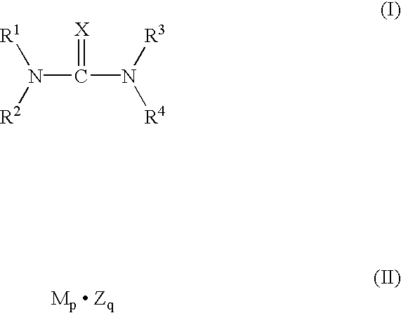
Further, Comparative Electrode T-1' was prepared in the same manner as the Comparative Electrode T-1 except that to the dye adsorption solution was added the compound (II-1), lithium iodide. Concentration of the compound (II-1) in the dye adsorption solution was 0.01 mol / l.
(2) Treatment Electrode
Electrodes T-3 to T-11 were prepared in the same manner as the Comparative Electrode T-1 except that the semiconductor fine particle was treated with the compound (I) and the compound (II) shown in Table 6, respectively.
(a) Pre-Treatment
In the production of the electrode T-7, pre-treatment using the compound (II-1) was carried out as follows. The coati...
PUM
| Property | Measurement | Unit |
|---|---|---|
| temperature | aaaaa | aaaaa |
| light transmittance | aaaaa | aaaaa |
| light transmittance | aaaaa | aaaaa |
Abstract
Description
Claims
Application Information
 - R&D
- Intellectual Property
- Life Sciences
- Materials
- Tech Scout
- Unparalleled Data Quality
- Higher Quality Content
- 60% Fewer Hallucinations
Browse by: Latest US Patents, China's latest patents, Technical Efficacy Thesaurus, Application Domain, Technology Topic, Popular Technical Reports.
© 2025 PatSnap. All rights reserved.Legal|Privacy policy|Modern Slavery Act Transparency Statement|Sitemap|About US| Contact US: help@patsnap.com


