Method for making low-resistance silicide contacts between closely spaced electrically conducting lines for field effect transistors

a field effect transistor and closely spaced electrical conductor technology, applied in the direction of basic electric elements, semiconductor devices, electrical apparatus, etc., can solve the problems of slowplasma etch rate, difficult to form reliable low-resistance and difficult to form good ohmic contacts to the source/drain contact area

Inactive Publication Date: 2002-09-17
TAIWAN SEMICON MFG CO LTD
View PDF11 Cites 22 Cited by
  • Summary
  • Abstract
  • Description
  • Claims
  • Application Information

AI Technical Summary

Problems solved by technology

Unfortunately, when the conformal insulating layer, typically SiO.sub.2, is etched back, the plasma etch rate is slower between the closely spaced gate electrodes, which makes it difficult to form reliable low-resistance ohmic contacts to the source / drain contact areas.
However, this oxide residue 16' makes it difficult to form good ohmic contacts to the source / drain contact areas 19(N+).
Typically the residual oxide 16' is removed by using an extended wet etch in a hydrofluoric (HF) acid solution, which can result in higher leakage currents and degrade the device characteristics.
However, none of the above references addresses the problems associated with residual silicon oxide between closely spaced gate electrodes resulting from slower etching in high-aspect openings, as described above.
Unfortunately in the conventional plasma etching process, the etch rate is slower between closely spaced lines because of the depletion effect of the etchant gas.
This slower etch rate results in residual SiO.sub.2 that makes it difficult to form good low-resistance ohmic silicide contacts for the FETs.
The amorphizing implant also modifies the top surface of the polysilicon gate electrodes, which reduces the sheet resistance when the silicide is formed on the gate electrodes.
The residual oxide 16' results in unreliable contacts to the substrate between the gate electrodes.

Method used


Image

  • Method for making low-resistance silicide contacts between closely spaced electrically conducting lines for field effect transistors
  • Method for making low-resistance silicide contacts between closely spaced electrically conducting lines for field effect transistors
  • Method for making low-resistance silicide contacts between closely spaced electrically conducting lines for field effect transistors

Examples


Embodiment Construction

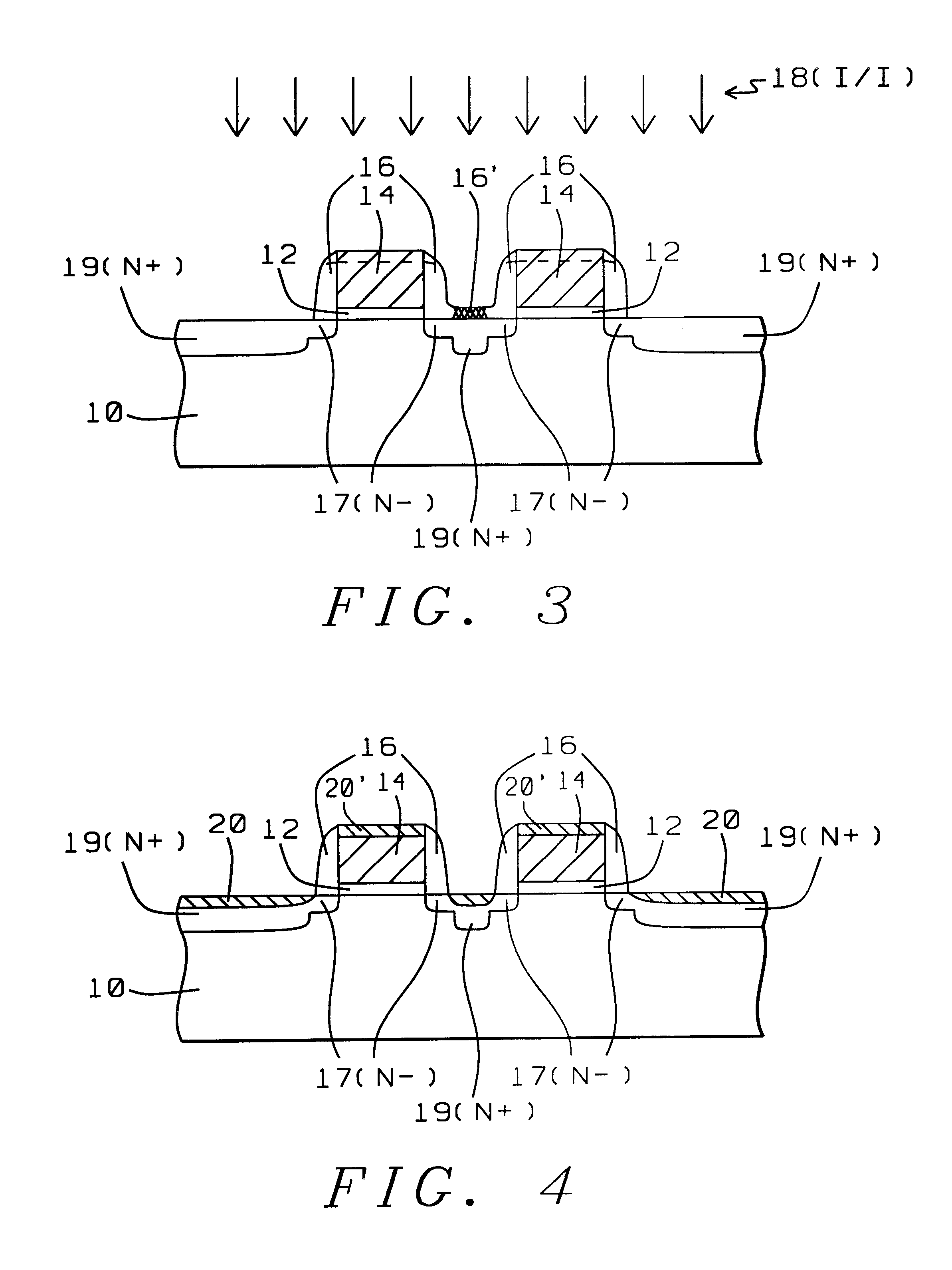
To better appreciate the advantages of this invention, FET structures were fabricated with closely spaced gate electrodes according to the description in the specification. The width of the gate electrodes was 0.25 um and the spacings, after forming the sidewall spacers, were 0.1 um. The sheet resistance (R.sub.s) in ohms / square was measured between the closely spaced gate electrodes and the cumulative percent yield was measured as a function of the R.sub.s. In FIG. 5 curve 2 is for P-channel FETs and for an amorphization implant with nitrogen (N) at a dose of 1.0 E 15 ions / cm.sup.2 and an implant energy of 10 KeV, and an implant angle normal to the surface. In FIG. 5 the y axis is the cumulative percent yield, and the x axis is the R.sub.s. Curve 3 is for an amorphization implant with germanium (Ge) at a dose of 3.0 E 14 ions / cm.sup.2 and an implant energy of 20 KeV, and an implant angle of 7 degrees from the normal to the surface. The R.sub.s by the method of this invention varies...


PUM


Abstract

A method for making reliable low-resistance contacts between closely spaced FET gate electrodes having high-aspect-ratio spacings. Polysilicon gate electrodes are formed. A conformal insulating layer is deposited and anisotropically etched back to form sidewall spacers on the gate electrodes. During conventional etch-back, the etch rate of the insulating layer between the closely spaced gate electrodes is slower resulting in a residual oxide that prevents the formation of reliable low-resistance contacts. This residual oxide requires an overetch in a hydrofluoric acid solution prior to forming silicide contacts. The wet overetch results in device degradation. A nitrogen or germanium implant is used to amorphize the oxide and to increase the wet etch rate of the residual oxide. Using this amorphization the wet etch that is commonly used as a pre-clean prior to forming silicide contacts can be used to remove the residual silicon oxide without overetching. The implant also results in a smoother interface between the silicide and the silicon substrate, which results in lower sheet resistance.

Description

BACKGROUND OF THE INVENTIONS(1) Field of the InventionThe present invention relates to the fabrication of integrated circuit devices on semiconductor substrates, and more particularly relates to a method for making reliable low-resistance silicide contacts between closely spaced patterned conducting stripes, hereafter also referred to as conducting lines. The method is particularly applicable for making more reliable silicide (source / drain) contacts between closely spaced sub-quarter-micrometer polysilicon gate electrodes (=or<0.25 um) for FETs. An ion implantation is used to amorphize any remaining residual silicon oxide (SiO.sub.2) between the polysilicon gate electrodes during formation of sidewall spacers. The amorphized oxide is then more rapidly removed in a wet etch, avoiding overetching that would cause device degradation.(2) Description of the Prior ArtAdvances in the semiconductor process technologies in recent years have dramatically decreased the device feature sizes ...

Claims


Application Information

Patent Timeline
IPC IPC(8): H01L21/336H01L21/02H01L21/285H01L21/3115
CPCH01L21/28518H01L29/665H01L21/31155
Inventor WANG, MEI-YUNJENG, SHWANGMINGSHUE, SHAU-LIN
Owner TAIWAN SEMICON MFG CO LTD
Why Eureka
Try Eureka