Configure registers and loads to tailor a multi-level cell flash design
a configuration register and multi-level technology, applied in the field of multi-level memory testing, can solve the problems of non-volatile memory manufacturing and operation, generally not reversible, time-consuming metal option methods,
- Summary
- Abstract
- Description
- Claims
- Application Information
AI Technical Summary
Benefits of technology
Problems solved by technology
Method used
Image
Examples
Embodiment Construction
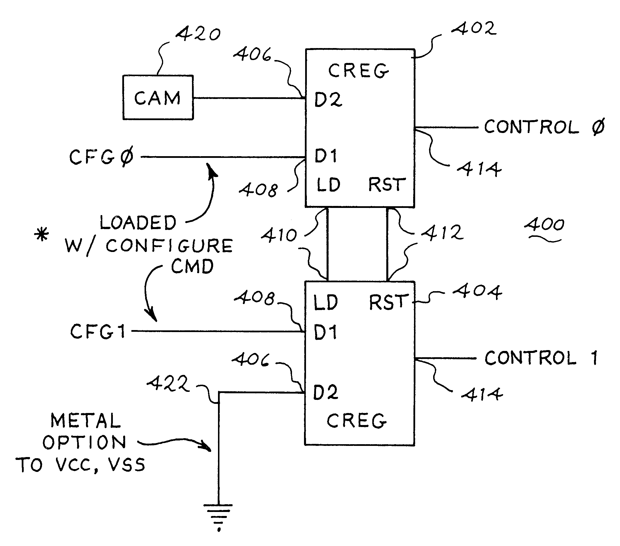
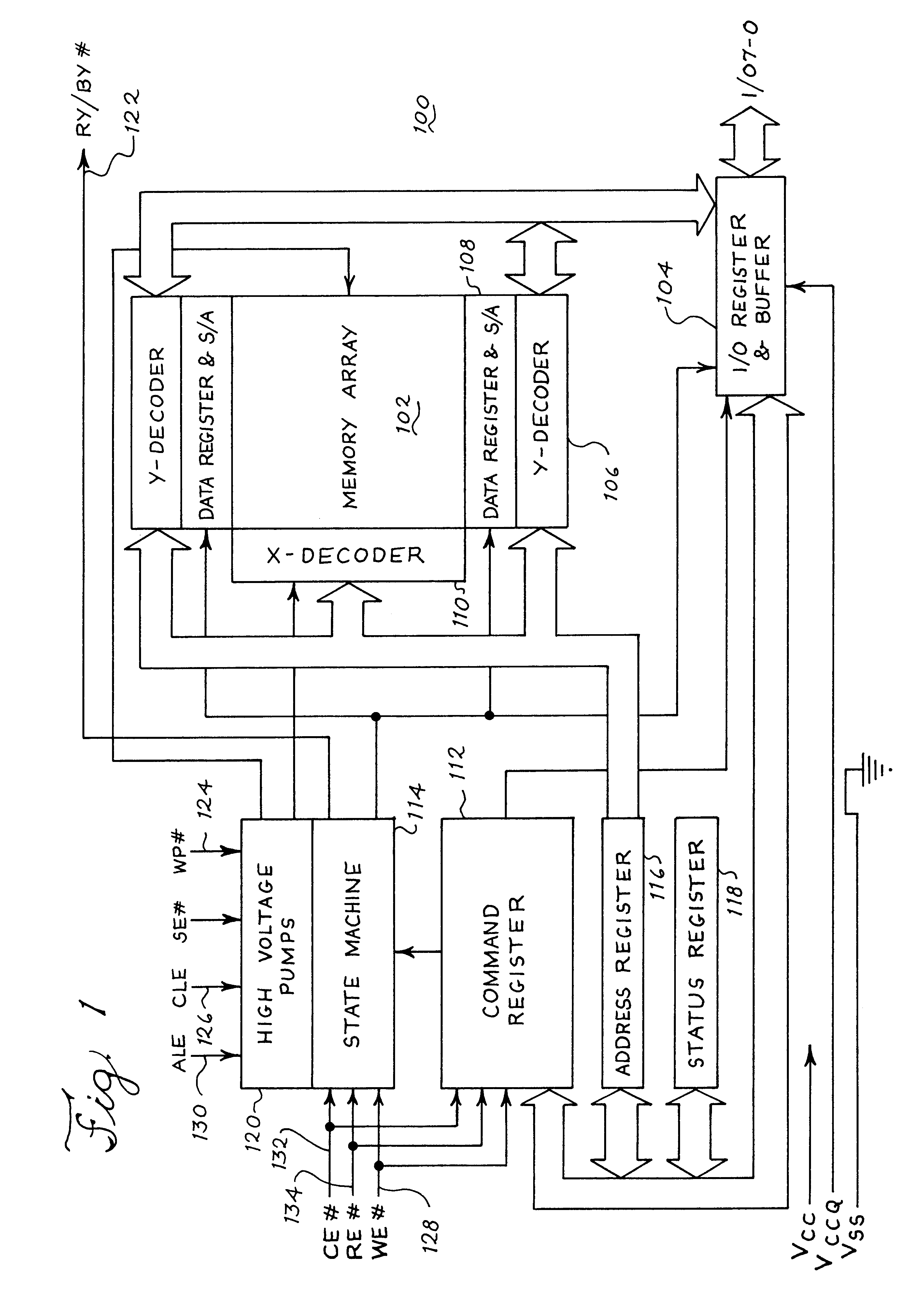
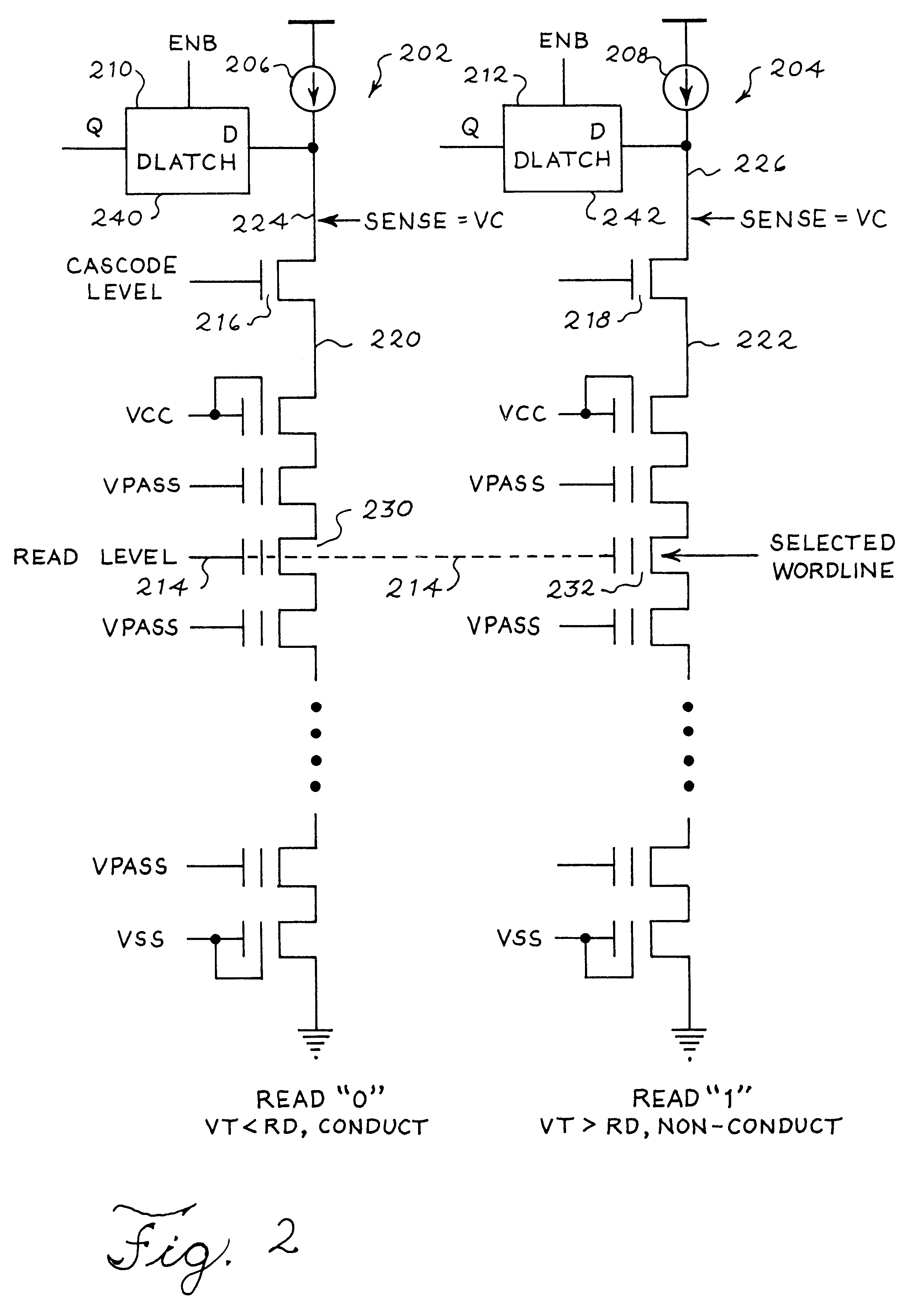
Referring now to the drawing, FIG. 1 shows a block diagram of a memory device 100. The memory device 100 in the illustrated embodiment is a NAND flash memory. However, in other embodiments, the memory device 100 may be any other suitable type of volatile memory such as random access memory (RAM) including static or dynamic RAM or nonvolatile memory such as EEPROM. Further, the memory device 100 may be an embedded memory circuit within another integrated circuit or device containing other circuitry, such as logic. As a flash memory, the memory device 100 may be written or programmed with data, read to retrieve the stored data, and erased to clear the memory device on a block-by-block basis.
In the illustrated embodiment, the memory device 100 includes a memory cell array 102, an input / output (I / O) register 104, one or more Y-decoders 106, one or more sense amplifier blocks 108 and one or more X-decoders 110. Further, the memory device 100 includes a command register 112, a state machi...
PUM
 Abstract
Description
Claims
Application Information
 - R&D
- Intellectual Property
- Life Sciences
- Materials
- Tech Scout
- Unparalleled Data Quality
- Higher Quality Content
- 60% Fewer Hallucinations
Browse by: Latest US Patents, China's latest patents, Technical Efficacy Thesaurus, Application Domain, Technology Topic, Popular Technical Reports.
© 2025 PatSnap. All rights reserved.Legal|Privacy policy|Modern Slavery Act Transparency Statement|Sitemap|About US| Contact US: help@patsnap.com


