Low-EMI electronic apparatus, low-EMI circuit board, and method of manufacturing the low-EMI circuit board.

a technology of electronic equipment and circuit boards, applied in the direction of sustainable manufacturing/processing, line-transmission details, final product manufacturing, etc., can solve the problems of increasing the number of electromagnetic environments, increasing the number of countermeasures for electronic products, and increasing the severity of electromagnetic environments

Inactive Publication Date: 2002-03-05
HITACHI LTD
View PDF22 Cites 184 Cited by
  • Summary
  • Abstract
  • Description
  • Claims
  • Application Information

AI Technical Summary

Benefits of technology

The present invention aims to suppress the spurious radiation at the level of the circuit board, and it eliminates various countermeasure parts such as a common mode choke, a filter and a bypass capacitor for an I / O unit and a power code which have been required in the prior art, and solves the problems of 1+L the increase of cost of the electronic apparatus, 2+L problems to so-called high packaging density such as minituarization, thinning and weight reduction of the product due to the increase of volume, 3+L the complexity of the countermeasure parts, and 4+L the restriction to the external design.
Further, since a design without the shield structure having plating applied to the plastic housing as seen in the modern notebook type personal computer is allowed, the shield structure is eliminated and 1+L the reduction of cost and 2+L the recycling of the plastic housing may be attained.
By providing the prior art countermeasure parts in the electronic apparatus of the present invention, it is natural to cope with the future increase of the spurious radiation and provide a highly reliable electronic apparatus against the spurious radiation.
In the structure or the circuit board of the present invention, in FIG. 14, in order to absorb the potential fluctuation V1 generated between the power layer (V) and the ground layer (G), a resistor Rc formed in the circuit board is connected to the capacitor C1 to form a parallel circuit (see FIG. 2) or a series circuit (see FIG. 12) of the capacitor C1 and the resistor Rc to reduce a Q value (attain Q value of not larger than 10).
Further, in the above structure, when the first dielectric material layer and the second dielectric material layer are formed by the same dielectric material, the warp of the circuit board may be reduced.

Problems solved by technology

Recently, the rise of an operating frequency due to high performance of a product raises a radiation intensity of spurious radiation, which leads the EMI to a severe situation.
Further, with the population of the electronic products, the countermeasure for the EMI of the electronic products is becoming severer.
If the spurious radiation increases in this manner, the electromagnetic environment becomes more and more worse and it is no doubt that a television video screen is disturbed or a manipulation system of an aircraft becomes uncontrollable and social problems are raised.
In order to enhance the EMC performance of the product, various countermeasure parts such as a common mode choke, a filter and a bypass capacitor for an I / O unit and a power supply have been used from the past but these parts present demerits of 1+L increase of a cost, 2+L problem to so-called high packaging density such as minituarization, thinning and weight reduction of a product due to the increase of volume, 3+L complexity of the countermeasure part, and 4+L restriction to external view design.
Further, in such a prior art product, the conformity to the future increase of the spurious radiation due to the rise of the operation frequency of the product is restricted.
However, since the inductances L0 and L1 due to the wiring pattern and the through-holes for connecting the bypass capacitor C0 are included by the nature of the circuit board structure, a resonance loop is created with the stray capacity C1 and the effective suppression of the potential fluctuation may be difficult.
Namely, as the operating frequency of the electronic product rises, the prior art technique cannot cope with the future increase of the spurious radiation.
As other countermeasure means, plating may be applied to a plastic housing to form a shield structure to suppress the spurious radiation as seen in a modern notebook type personal computer, but the shield structure has demerits of 1+L increase of cost and 2+L the reduction of added value of the product by a problem to recycling the plastic housing.
Thus, new countermeasure means for suppressing the spurious radiation without lowering the added value of the electronic apparatus has been demanded, and on the other hand, a mechanism of the spurious radiation has not been fully investigated.

Method used


Image

  • Low-EMI electronic apparatus, low-EMI circuit board, and method of manufacturing the low-EMI circuit board.
  • Low-EMI electronic apparatus, low-EMI circuit board, and method of manufacturing the low-EMI circuit board.
  • Low-EMI electronic apparatus, low-EMI circuit board, and method of manufacturing the low-EMI circuit board.

Examples


Embodiment Construction

The embodiments of the present invention are now explained.

FIG. 33 shows an external view of an electronic apparatus (personal computer) using a low EMI circuit board in accordance with one embodiment of the present invention.

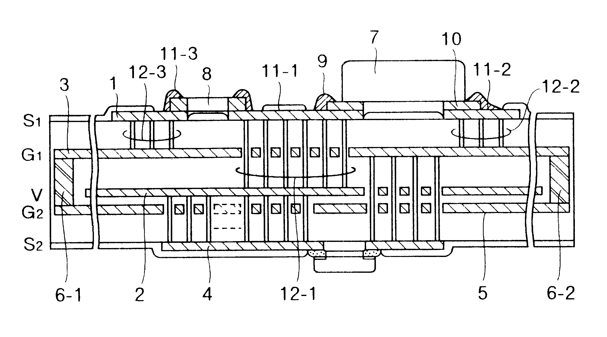
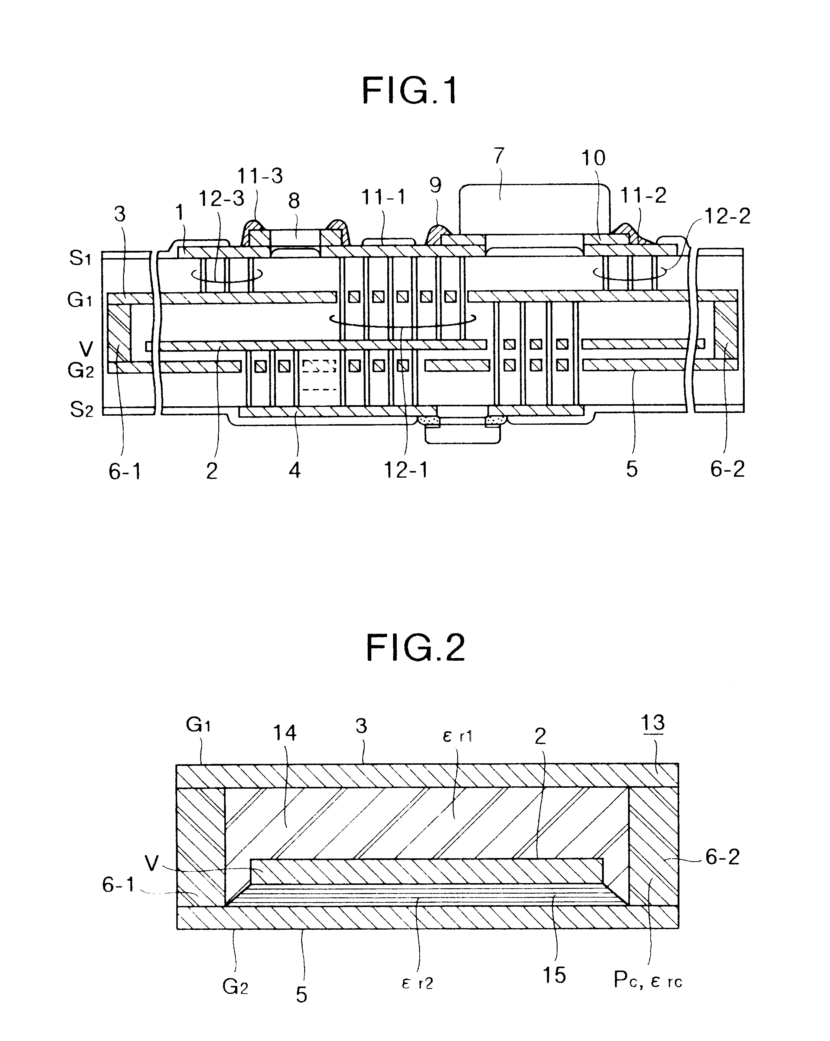
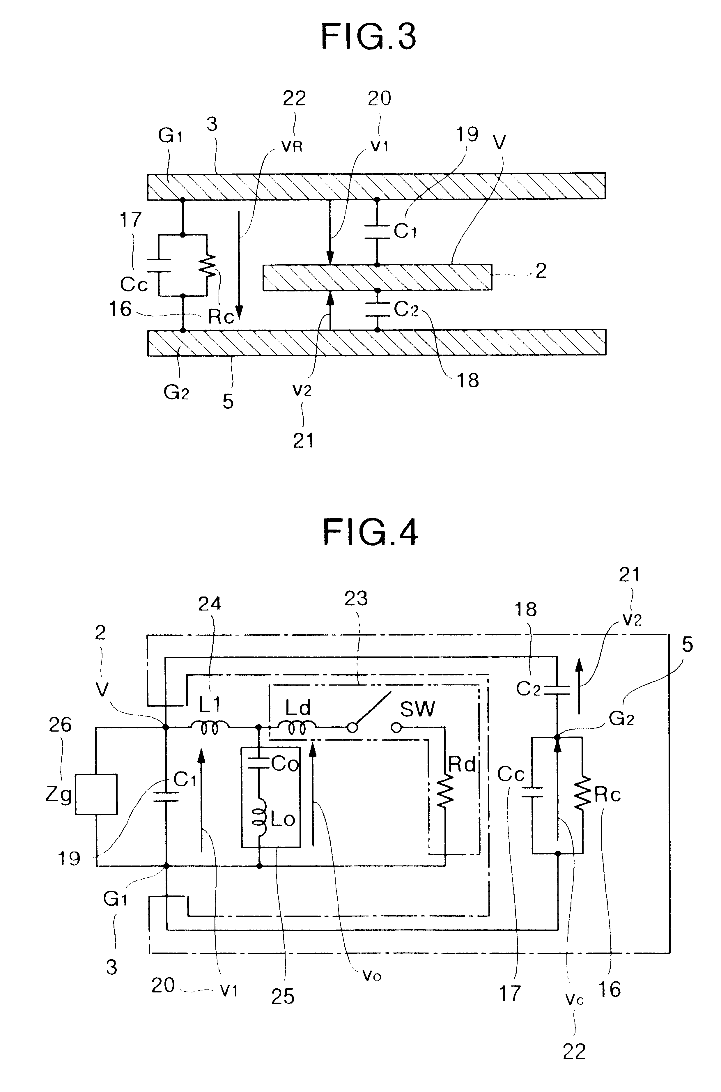
In the electronic apparatus 1 of the present invention, components comprising I / O connectors 4 (4-1, . . . , 4-5), a power code 5, a signal cable 6, a housing 7, an LCD display 8, a keyboard 9, a floppy disk drive 10, a hard disk drive 11, a battery pack 12 and an IC card 13 are electrically and physically connected around a low EMI circuit board 3 on which a high speed CPU 2 is mounted. The low EMI circuit board 3 comprises "first and second ground layers having at least one thereof electrically connected to electrical parts, a power layer provided between said first ground layer and said second ground layer and electrically connected to said electronic parts, a dielectric material layer for joining said second ground layer and said power layer and a resistor ...


PUM

PropertyMeasurementUnit
operating frequencyaaaaaaaaaa
dielectric constantsaaaaaaaaaa
thicknessaaaaaaaaaa

Abstract

A low-EMI circuit which realizes a high mounting density by converting the potential fluctuation off a power supply layer with respect to a ground layer which occurs on switching an IC device etc., into Joule's heat in the substrate without using any parts as a countermeasure against the EMI. Its structure, a circuit board using it, and a method of manufacturing the circuit board are also disclosed. Parallel plate lines in which the Q-value of the stray capacitance between solid layers viewed from the power supply layer and ground layer is equivalently reduced and which are matchedly terminated by forming a structure in which a resistor (resistor layer) and another ground layer are provided in addition to the power supply layer and the ground layer on a multilayered circuit board. A closed shield structure is also disclosed. This invention can remarkably suppress unwanted radiation by absorbing the potential fluctuation (resonance) which occurs in a power supply loop by equivalently reducing the Q-value of the stray capacitance, absorbing the standing wave by the parallel plate lines matchedly terminated and, closing and shielding the parallel plate lines.

Description

The present invention relates to an electronic apparatus which copes with an EMC which is becoming more and more important in increasing speed and packaging density of IC and LSI devices, and to a device, a circuit board and an electronic apparatus which require suppression means for spurious radiation noise and a method of making the same.An EMC intends to the compatibility of an electromagnetic environment of an EMI (noise source) and an immunity (noise receiver). Recently, the rise of an operating frequency due to high performance of a product raises a radiation intensity of spurious radiation, which leads the EMI to a severe situation. Further, with the population of the electronic products, the countermeasure for the EMI of the electronic products is becoming severer.It is reported that the increase of the anticipated spurious radiation amounts to 4 dB / year. If the spurious radiation increases in this manner, the electromagnetic environment becomes more and more worse and it is...

Claims


Application Information

Patent Timeline
Patent Type & Authority Patents(United States)
IPC IPC(8): H01L23/52H01L23/552H01L23/538H01L25/16H05K9/00H05K1/02H05K1/16H05K3/42H05K3/46H05K1/11H05K3/40H05K1/09
CPCH01L23/5383H01L25/16H05K1/0234H05K1/0246H05K1/167H05K9/0039H01L23/552Y10T29/49155H01L2224/16H01L2924/01046H01L2924/01057H01L2924/01078H01L2924/01079H01L2924/09701H01L2924/16152H01L2924/19105H01L2924/19106H01L2924/3011H01L2924/3025H05K1/0227H05K1/0231H05K1/092H05K1/113H05K1/115H05K1/162H05K3/403H05K3/4053H05K3/429H05K3/4611H05K3/4614H05K3/4652H05K3/467H05K2201/0209H05K2201/0715H05K2201/093H05K2201/09309H05K2201/09354H05K2201/09509H05K2201/09518H05K2201/09563H05K2201/09663H05K2201/0979H05K2201/10022H05K2201/10045H05K2201/10446H05K2201/10636H05K2201/10689H01L2924/01019H01L2924/00014Y02P70/50H01L2224/0401H05K3/46
Inventor AKIBA, YUTAKANARIZUKA, YASUNORITANEI, HIRAYOSHIKITAMURA, NAOYA
Owner HITACHI LTD
Why Eureka
Try Eureka