
Method for stripping organic based film

a technology stripping method, which is applied in the field of organic based film, can solve the problems of increasing the -layer capacitance, the increase of the signal delay time, and the manufacture of such high-integrated ultras

Inactive Publication Date: 2002-03-05
SONY CORP +1
View PDF5 Cites 16 Cited by
  • Summary
  • Abstract
  • Description
  • Claims
  • Application Information

AI Technical Summary

Benefits of technology

With the present method for stripping the organic film according to the present invention, the organic film is stripped by radicals generated in the gas mainly composed of a fluorine-based gas. These radicals are lower in reactivity with the organic low dielectric constant insulating film than with the organic film and hence are not reacted with the organic low dielectric constant insulating film. Thus, with the present technique, the organic film can be stripped from the organic low dielectric constant insulating film without the risk of ashing thereof.
By adding oxygen, the radical generating reaction for the fluorine-based gas is accelerated to permit radicals to react efficiently with the organic film.
In this case, by adding the inert gas, it is possible to control ammonia to desired concentration and hence to control the amount of yielded radicals. Thus, with this technique, the organic film can be stripped with a controlled stripping rate.
In this stripping method for the organic film according to the present invention, part of the organic film is first stripped by radicals generated in the gas mainly composed of the fluorine gas, and the remaining portion of the organic film is stripped by radicals generated in the gas mainly composed of ammonia. That is, with the technique, the organic low dielectric constant insulating film is ashed in two separate steps. First, the organic film is ashed by radicals generated in the gas mainly composed of the fluorine-based gas. Subsequently, the remaining portion of the organic film is completely stripped by radicals generated in the gas mainly composed of ammonia. This technique permits complete stripping of the organic film formed on the layered unit.
With the method for stripping the organic film according to the present invention, the organic film can be positively removed without the risk of stripping the organic low dielectric constant insulating film, because of the low reactivity between radicals removing the organic film and the organic low dielectric constant insulating film. Thus, with this technique, a semiconductor device having a desired shape can be manufactured without incurring the risk of etching the organic low dielectric constant insulating film.

Problems solved by technology

Since it is difficult to manufacture such highly integrated ultra LSI devices by simply miniaturizing the planar devices, a multi-layer interconnection structure of stacking the devices in plural layers is used.
However, with a device having the multi-layer interconnection structure, the inter-layer capacitance in the multi-layer interconnection structure is increased, as a result of which the signal delay time is also increased.
However, this SiOF film, low in dielectric constant among inorganic based materials, has a dielectric constant .di-elect cons. of the order of 3.5, such that it cannot sufficiently reduce the above-mentioned interlayer capacitance.
Therefore, the inorganic-based low dielectric constant insulating film is thought to be insufficient for use as an inter-layer film in the ultra-LSI device.
These protective layers reduce the effect of the organic low dielectric constant insulating film on the interconnection layer.
However, since the organic low dielectric constant insulating film is formed of an organic material similar to the resist mask material, it is a frequent occurrence that the organic low dielectric constant insulating film is ashed together with the resist mask.
That is, this technique experiences a problem that a device having an organic low dielectric constant insulating film cannot be processed to a desired shape.

Method used


Image

  • Method for stripping organic based film
  • Method for stripping organic based film

Examples


Embodiment Construction

Referring to the drawings, preferred embodiments of the method for stripping an organic film according to the present invention will be explained in detail.

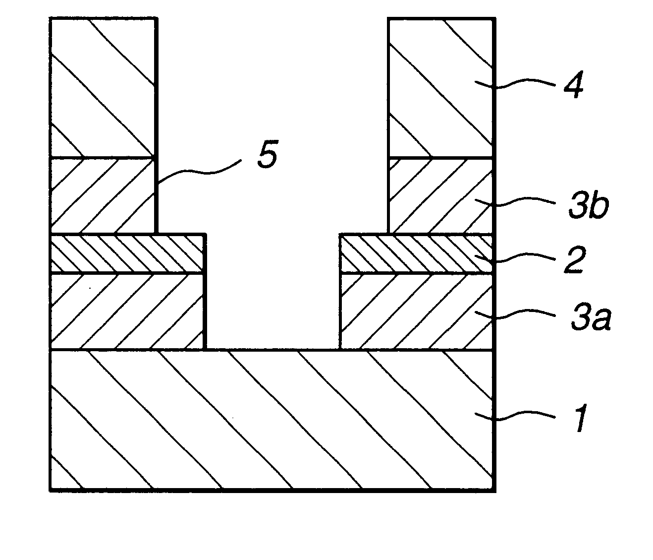
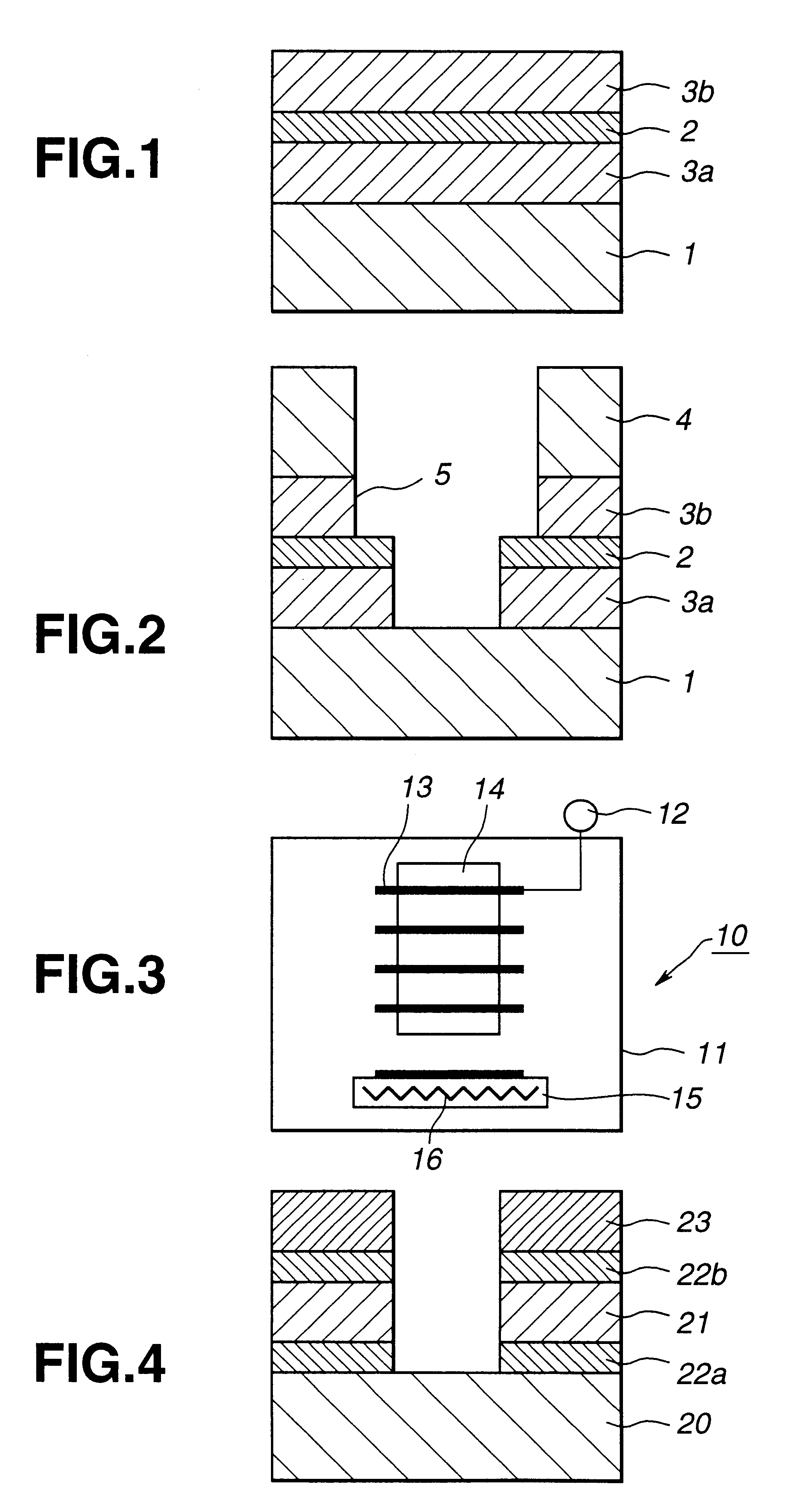
The method for stripping the organic film according to the present invention is used for stripping an organic film formed on a layered unit having an organic low dielectric constant insulating film. In the present invention, the layered unit having the organic low dielectric constant insulating film includes a pair of organic low dielectric constant insulating films 3a, 3b formed on a lower interconnection film 1 for sandwiching a Sl.sub.3 N.sub.4 film 2 in-between.

With the layered unit constructed as described above, an organic film 4 is formed to a pre-set shape on the upper organic low dielectric constant insulating film 3b, and a connection hole 5 is formed using this organic film 4 as a resist mask. This connection hole 5 is formed by boring in the layered unit exposed from the organic film 4 to a depth sufficient to expose ...


PUM

PropertyMeasurementUnit
dielectric constantaaaaaaaaaa
temperatureaaaaaaaaaa

Abstract

There is provided a method used for processing an organic low dielectric constant insulating film to a desired shape for enabling facilitated stripping of an organic film formed on top of the organic low dielectric constant insulating film. Specifically, there is provided a method for stripping an organic film formed on a layered unit having at least an organic low dielectric constant insulating film. This method includes generating radicals in a gas mainly composed of fluorine-based gas, and stripping the organic film by the generated radicals.

Description

1. Field of the InventionThis invention relates to an organic-based film, such as a resist film, formed on a layered unit having an organic-based low dielectric constant film exhibiting high reactivity to an oxygen plasma.2. Related ArtAn ultra-LSI device is demanded for integrating millions or more of devices on a chip each side of which measures only several mm. Since it is difficult to manufacture such highly integrated ultra LSI devices by simply miniaturizing the planar devices, a multi-layer interconnection structure of stacking the devices in plural layers is used. This multi-layer interconnection structure is indispensable in manufacturing a highly integrated ultra LSI.The ultra LSI is also demanded for a high device function and a higher operating speed, and hence the prompt development of semiconductor forming process technique satisfying this demand is mandatory. The above-mentioned multi-layer interconnection technique may be mentioned as one of the types of the semicond...

Claims


Application Information

Patent Timeline
Patent Type & Authority Patents(United States)
IPC IPC(8): H01L21/02H01L21/311H01L21/312H01L21/302G03F7/42H01L21/027H01L21/3065
CPCH01L21/3127H01L21/31138H01L21/0212
Inventor KADOMURA, SHINGOWONG, JERRYTOSHIMA, MASATO
Owner SONY CORP
Learn More