Memory test device and method capable of achieving fast memory test without increasing chip pin number
a test device and memory technology, applied in measurement devices, error detection/correction, instruments, etc., can solve the problems of difficult to achieve, inability to achieve the test of memory, and requiring a more expensive tester and pins
- Summary
- Abstract
- Description
- Claims
- Application Information
AI Technical Summary
Problems solved by technology
Method used
Image
Examples
embodiment 1
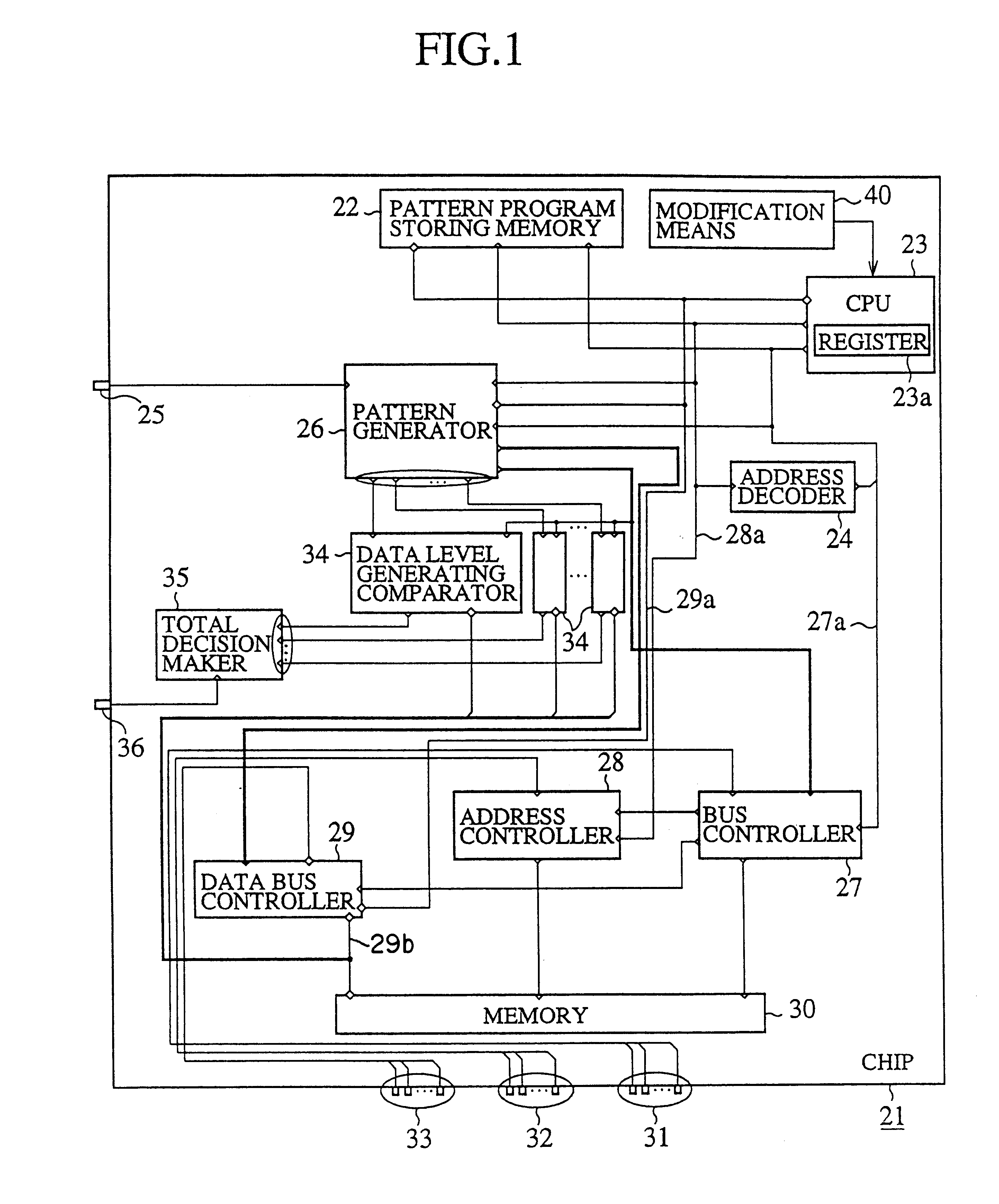
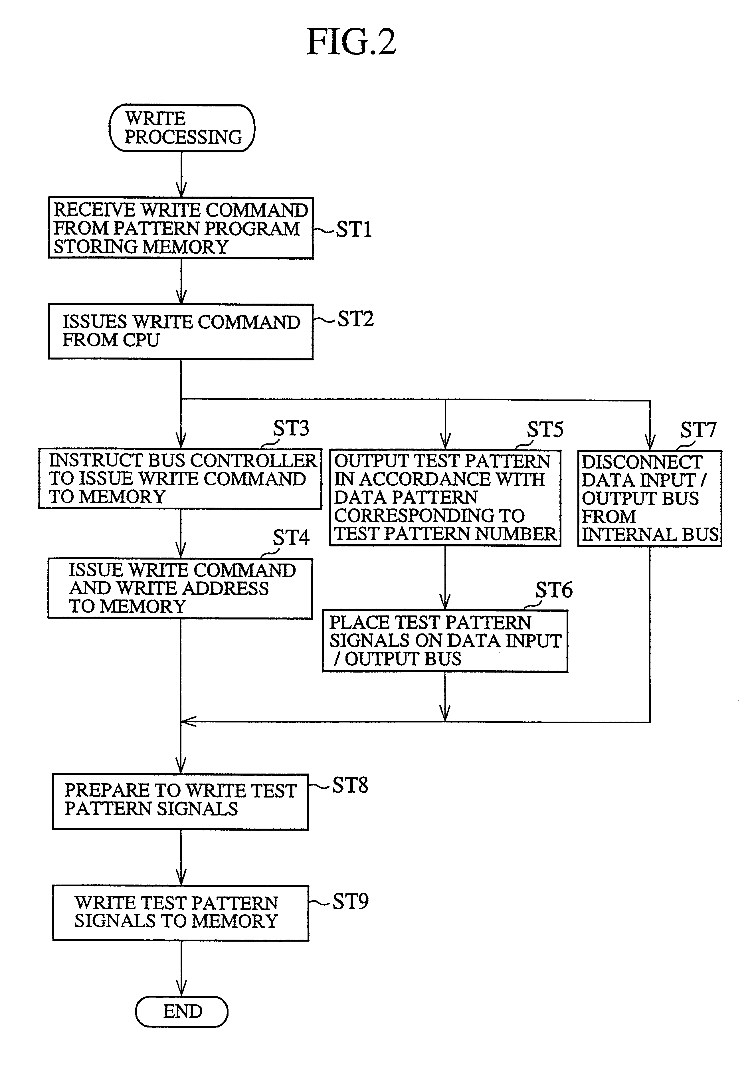
FIG. 1 is a block diagram showing a configuration of a memory test device in accordance with the present invention. In FIG. 1, the reference numeral 21 designates a chip that mounts a memory 30 to be tested; and 22 designates a pattern program storing memory (issue means, pattern number issue means, program issue means, and a pattern number issue procedure memory) that stores a pattern program, a write command including a test pattern number and the like. The pattern program stores process control instructions such as a jump command and a loop counter command, which control the flow of the memory test; stores an address increment / decrement command for controlling the write or read address of the test pattern, which is stored in a register 23a of a CPU 23, an issue command for issuing the write command including the test pattern number, and other instructions needed for the memory test.
The reference numeral 23 designates the CPU (issue means, pattern number issue means, and program i...
embodiment 2
Although the CPU 23 issues the write command including the test pattern number in the foregoing embodiment 1, the CPU 23 can issue a write command including a data pattern, achieving an effect similar to that of the foregoing embodiment 1.
More specifically, the pattern program storing memory 22 stores the write command including the data pattern, and the CPU 23 issues the write command including the data pattern. The pattern generator 26, without having the internal memory for storing the data pattern, outputs the test pattern in accordance with the data pattern supplied from the CPU 23.
Although the time period the CPU 23 occupies the data input / output bus 29b becomes a little longer than that in the foregoing embodiment 1 because the amount of data of the write command including the data pattern is greater than that of the write command including the test pattern number, the internal memory of the pattern generator 26 can be removed, and the selection becomes unnecessary of the dat...
embodiment 3
Although the foregoing embodiments 1 and 2 do not modify the data patterns stored in the internal memory of the pattern generator 26 or the pattern program stored in the pattern program storing memory 22, the modification means 40 can be provided for modifying the data patterns or the pattern program (see, FIG. 1).
This makes it easier to generate a variety of test patterns, offering an advantage of being able to implement various types of memory tests.
In addition, storing all of or part of the pattern program storing memory 22 in a ROM or flash memory makes it possible to implement a test during power-up after mounting the chip on a real product.
PUM
 Abstract
Description
Claims
Application Information
 - R&D
- Intellectual Property
- Life Sciences
- Materials
- Tech Scout
- Unparalleled Data Quality
- Higher Quality Content
- 60% Fewer Hallucinations
Browse by: Latest US Patents, China's latest patents, Technical Efficacy Thesaurus, Application Domain, Technology Topic, Popular Technical Reports.
© 2025 PatSnap. All rights reserved.Legal|Privacy policy|Modern Slavery Act Transparency Statement|Sitemap|About US| Contact US: help@patsnap.com


