
Method of forming metal layer using atomic layer deposition and semiconductor device having the metal layer as barrier metal layer or upper or lower electrode of capacitor

a metal layer and atomic layer technology, applied in chemical vapor deposition coatings, coatings, capacitors, etc., can solve the problems of inability to adjust and reproduce composition, inability to act as barrier metal layers, and increased complexity of structur

Inactive Publication Date: 2001-09-11
SAMSUNG ELECTRONICS CO LTD
View PDF3 Cites 1122 Cited by
  • Summary
  • Abstract
  • Description
  • Claims
  • Application Information

AI Technical Summary

Benefits of technology

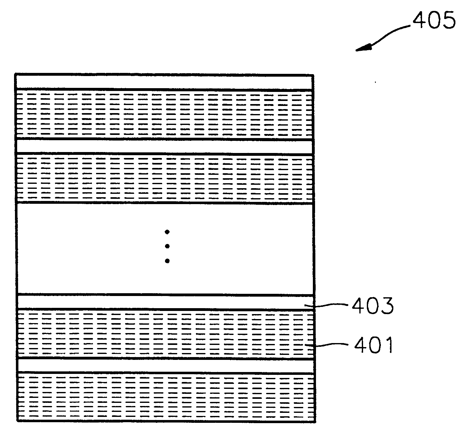
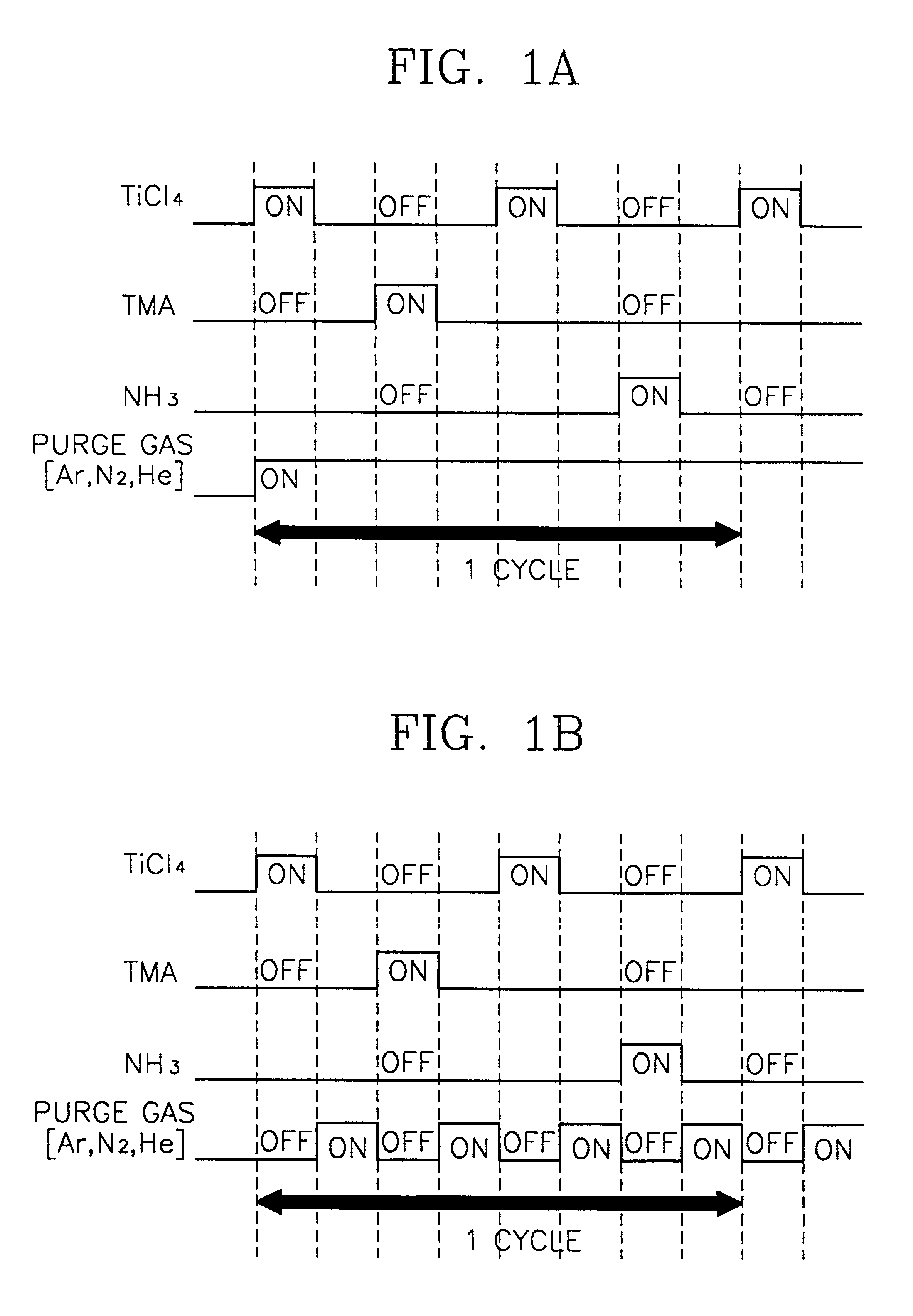
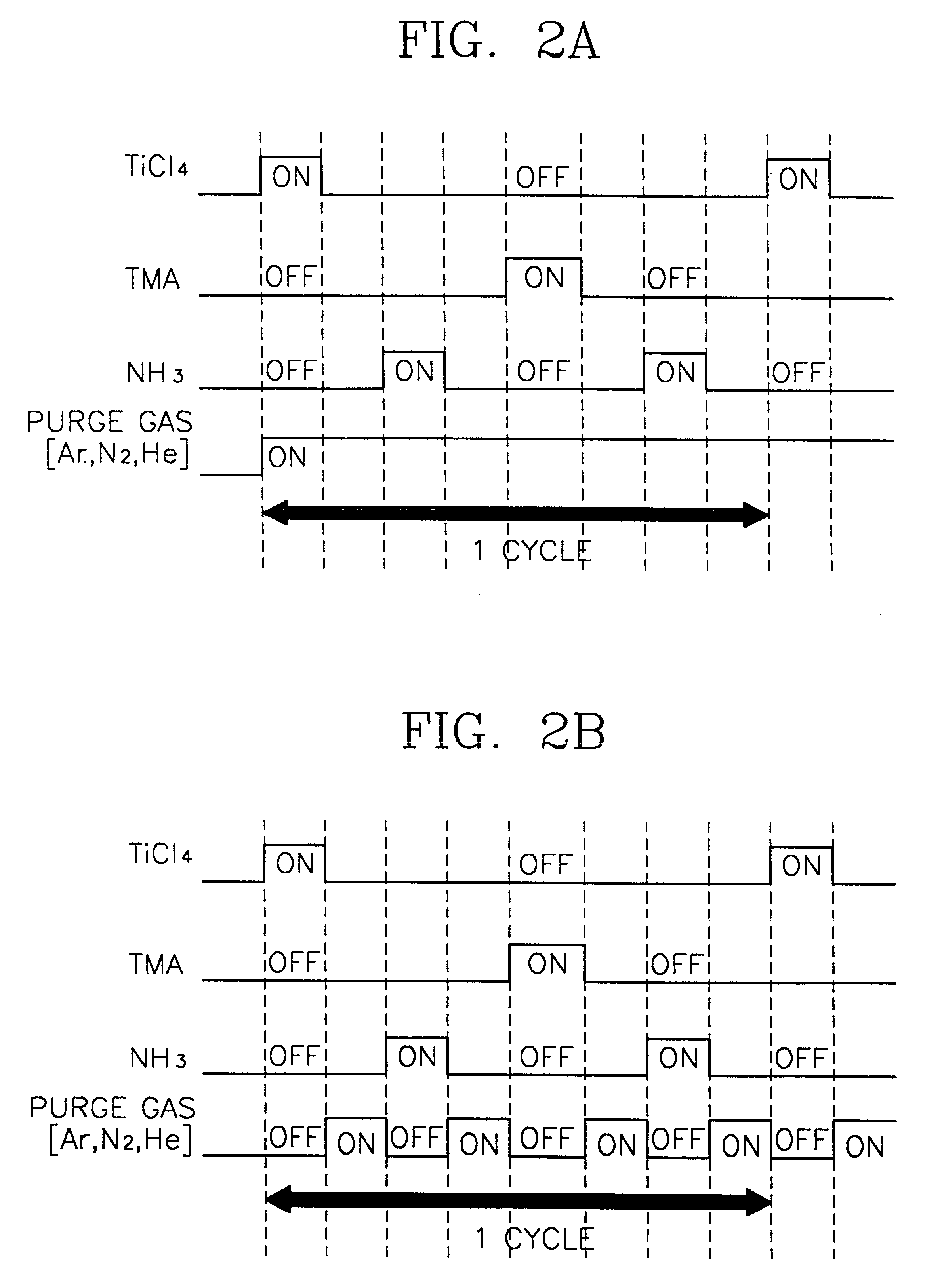
Accordingly, to achieve the first object, the present invention by a first aspect provides a method of forming a metal layer having an A--B--N structure in which a plurality of atomic layers are stacked by individually injecting pulsed source gases for a reactive metal (A), an amorphous combination element (B) for preventing crystallization of the reactive metal (A) and nitrogen (N), and nitrogen (N) and allowing the source gases to be chemically adsorbed to a semiconductor substrate.
As described above, a metal layer (a multiple metal layer) formed by atomic layer deposition of the present invention has a high thermal resistant and high oxidation resistant characteristics. Since the metal layer is formed by individually depositing atomic layers, the step coverage thereof is excellent even in a very compact region. In addition, since individual atomic layers are adsorbed and formed in a predetermined order, the composition ratio of each element contained in the metal layer can be easily adjusted. A metal layer formed by atomic layer deposition of the present invention may be employed as a barrier metal layer, a lower electrode or an upper electrode in a semiconductor device.

Problems solved by technology

In addition, platinum (Pt) and silicon (Si) is diffused into the TiN film, and thus the TiN film cannot act as a barrier metal layer.
A barrier metal layer formed of a compound containing a refractory metal has a problem that adjustability and reproducibility of composition is decreased when the compound is deposited by chemical vapor deposition, due to the complexity of the composition.
However, a barrier metal layer formed by a sputtering process has a poor step coverage so that it cannot be suitable for a barrier metal layer in a capacitor, the structure of which becomes more complex as the integration density of a semiconductor device increases, for example, a barrier metal layer which is formed at the lower portion of a trench having a high aspect ratio in a trench type capacitor.

Method used


Image

  • Method of forming metal layer using atomic layer deposition and semiconductor device having the metal layer as barrier metal layer or upper or lower electrode of capacitor
  • Method of forming metal layer using atomic layer deposition and semiconductor device having the metal layer as barrier metal layer or upper or lower electrode of capacitor
  • Method of forming metal layer using atomic layer deposition and semiconductor device having the metal layer as barrier metal layer or upper or lower electrode of capacitor

Examples


second embodiment

With reference to FIGS. 8A through 8E, a cylinder type capacitor employing a metal layer formed by atomic layer deposition as an upper electrode will be described. Referring to FIG. 8A, an insulating layer 210 composed of a silicon oxide (SiO.sub.2) film is formed on a semiconductor substrate 104. Subsequently, photo etching is performed to form a contact hole in the insulating layer 210.

Referring to FIG. 8B, the contact hole is filled with a conductive material to form a plug 212. For example, the contact hole may be filled with doped polysilicon to form a poly plug.

Referring to FIG. 8C, a cylinder type lower electrode 214 composed of a metal such as Al or W is formed on the insulating layer 210 and the plug 212 using a photoresist pattern (not shown). Next, a barrier metal layer 216 is formed of TiN or TaN between the cylinder type lower electrode 214 and the poly plug 212 to prevent oxidation of the poly plug 212 during a later thermal process. When the lower electrode 214 is a m...

third embodiment

With reference to FIGS. 9A through 9E, a trench type capacitor employing a metal layer formed by atomic layer deposition as a lower electrode will be described. Referring to FIG. 9A, an insulating layer 310 composed of a silicon oxide (SiO.sub.2) film is formed on a semiconductor substrate 104. Subsequently, photo etching is performed to form a contact hole in the insulating layer 310.

Referring to FIG. 9B, the contact hole may be partially filled to a predetermined depth or not filled at all to give a desired capacitance. When partially filling the contact hole, the contact hole is filled with polysilicon and then wet etching or wet etching combined with chemical mechanical polishing is performed on the polysilicon to leave a polysilicon film 312 of a predetermined thickness at the bottom of the contact hole.

Referring to FIG. 9C, a lower electrode 314 is formed on the insulating layer 310 and on the polysilicon film 312. The lower electrode 314 is formed in a similar manner to that ...


PUM

PropertyMeasurementUnit
thicknessaaaaaaaaaa
thicknessaaaaaaaaaa
temperatureaaaaaaaaaa

Abstract

A method of forming a metal layer having excellent thermal and oxidation resistant characteristics using atomic layer deposition is provided. The metal layer includes a reactive metal (A), an element (B) for the amorphous combination between the reactive metal (A) and nitrogen (N), and nitrogen (N). The reactive metal (A) may be titanium (Ti), tantalum (Ta), tungsten (W), zirconium (Zr), hafnium (Hf), molybdenum (Mo) or niobium (Nb). The amorphous combination element (B) may be aluminum (Al), silicon (Si) or boron (B). The metal layer is formed by alternately injecting pulsed source gases for the elements (A, B and N) into a chamber according to atomic layer deposition to thereby alternately stack atomic layers. Accordingly, the composition ratio of a nitrogen compound (A-B-N) of the metal layer can be desirably adjusted just by appropriately determining the number of injection pulses of each source gas. According to the composition ratio, a desirable electrical conductivity and resistance of the metal layer can be accurately obtained. The atomic layers are individually deposited, thereby realizing excellent step coverage even in a complex and compact region. A metal layer formed by atomic layer deposition can be employed as a barrier metal layer, a lower electrode or an upper electrode in a semiconductor device.

Description

1. Field of the InventionThe present invention relates to a method of forming a metal layer using atomic layer deposition and a semiconductor device having the metal layer as a barrier metal layer or the upper or lower electrode of a capacitor.2. Description of the Related ArtAs the integration density of semiconductor devices increases, high dielectric materials having a large dielectric constant have been developed to obtain large capacitance in a small area. For example, a BST (BaSrTiO.sub.3) film having a perovskite crystal structure has a dielectric constant of about several hundreds through one thousand in a bulk state, which is different to a silicon nitride film, a silicon oxy-nitride film and a tantalum oxide (Ta.sub.2 O.sub.5) film which are conventionally used for a capacitor. A BST film is advantageous in that a thin dielectric film can be implemented such that an equivalent oxide thickness is less than 10 .ANG. even when the thickness of the BST film is more than 500 .A...

Claims


Application Information

Patent Timeline
Patent Type & Authority Patents(United States)
IPC IPC(8): C23C16/34H01L21/285H01L21/768H01L21/02H01L21/70C23C16/44C23C16/455
CPCC23C16/34C23C16/45529H01L21/28562H01L21/76843H01L28/75H01L21/76849H01L21/76865H01L21/7687H01L21/76846
Inventor KANG, SANG-BOMLIM, HYUN-SEOKCHAE, YUNG-SOOKJEON, IN-SANGCHOI, GIL-HEYUN
Owner SAMSUNG ELECTRONICS CO LTD
Learn More