
Simultaneous program, program-verify scheme

a program and program technology, applied in the field of simulation program and program verification operations, can solve the problems of high density, low power consumption, high performance, and inability to update in the system, and achieve the effect of reducing the cost of sram and dram

Inactive Publication Date: 2001-04-10
MONTEREY RES LLC
View PDF4 Cites 40 Cited by
  • Summary
  • Abstract
  • Description
  • Claims
  • Application Information

AI Technical Summary

Benefits of technology

By way of introduction only, the present invention provides simultaneous program and program-verify operations for a non-volatile memory device. In one preferred embodiment, a memory device is divided into two or more banks. Each bank includes a number of sectors. Each sector includes a set of memory cells. Each bank has a decod

Problems solved by technology

ROM memories have high density, low power consumption, and high performance, but they are not in-system updateable.
The RAM family, however, is in-system updateable and has high performance, but it is volatile.
SRAM is considerably more expensive than DRAM.
One problem with prior flash memories is that they do not provide sufficient random access.
For example, prior flash memory devices typically do not allow a processor to perform a program-verify operation while a program operation is underway in the memory device.
That is, a processor should wait until a program cycle is complete before initiating a program-verify cycle, because both program and program-verify operations cannot be performed simultaneously.
While prior art memory systems allow simultaneous read and write operations, they suffer from the problem that they can only do asynchronous (not clocked) memory read operation in combination with another embedded memory operation, such as embedded memory program or embedded memory erase operations.
Because asynchronous memory read operation is not a command-sequence-mode (embedded) operation, rather it is a direct-mode-operation like a default operation, prior art memory systems are not capable of simultaneously performing two command-sequence-mode (embedded) operations such as memory erase, memory write, and memory program-verify operations.

Method used


Image

  • Simultaneous program, program-verify scheme
  • Simultaneous program, program-verify scheme
  • Simultaneous program, program-verify scheme

Examples


Embodiment Construction

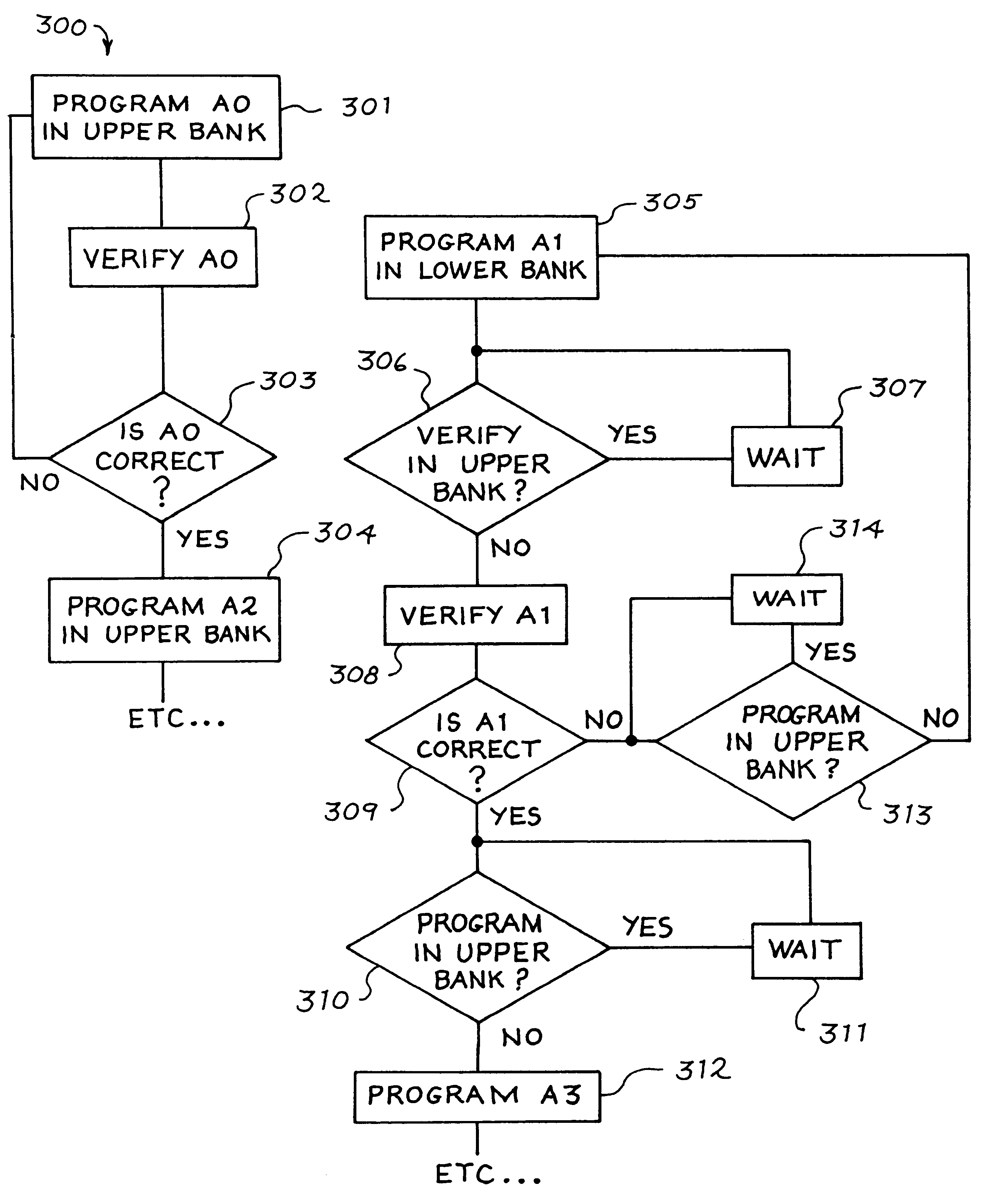
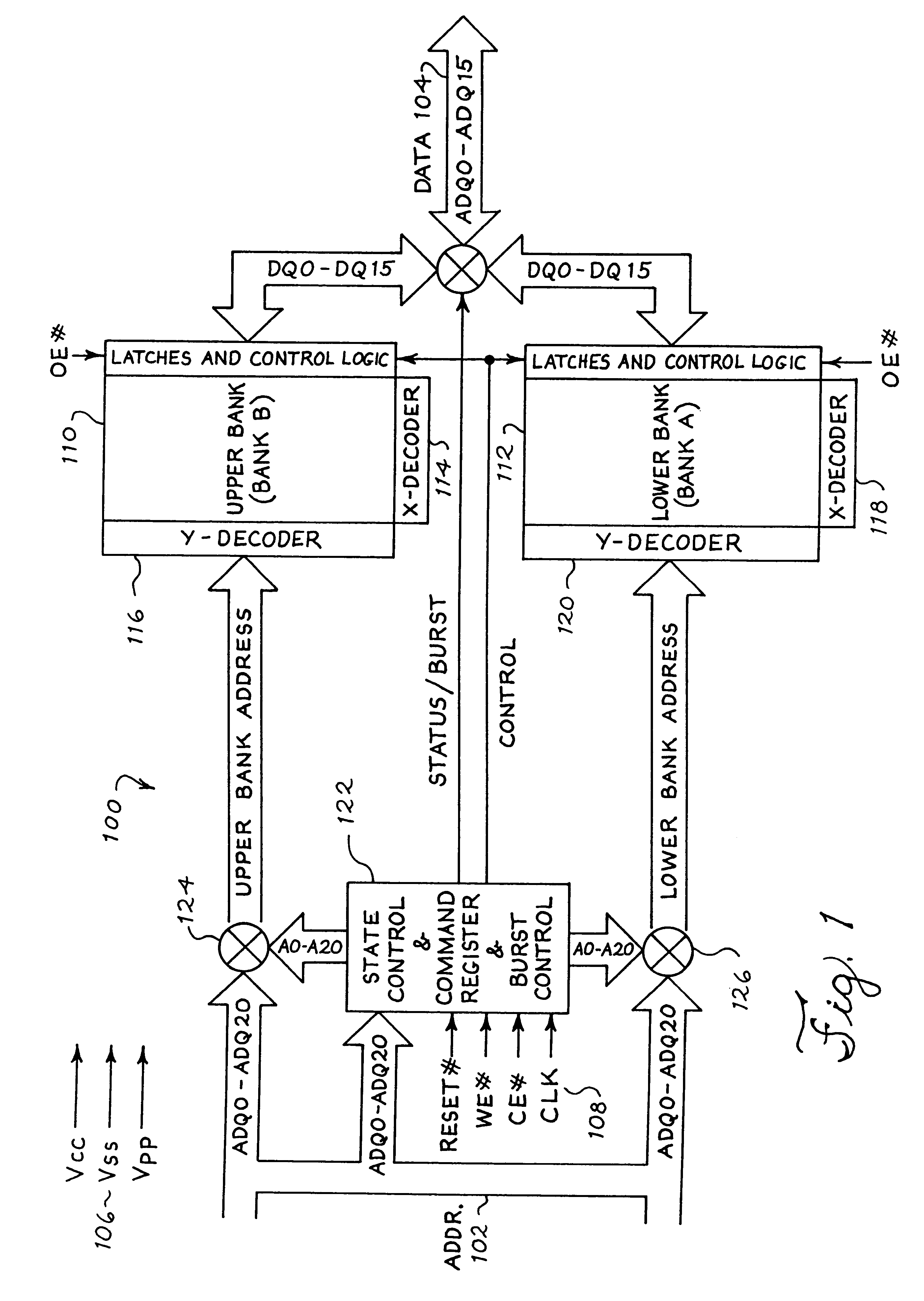
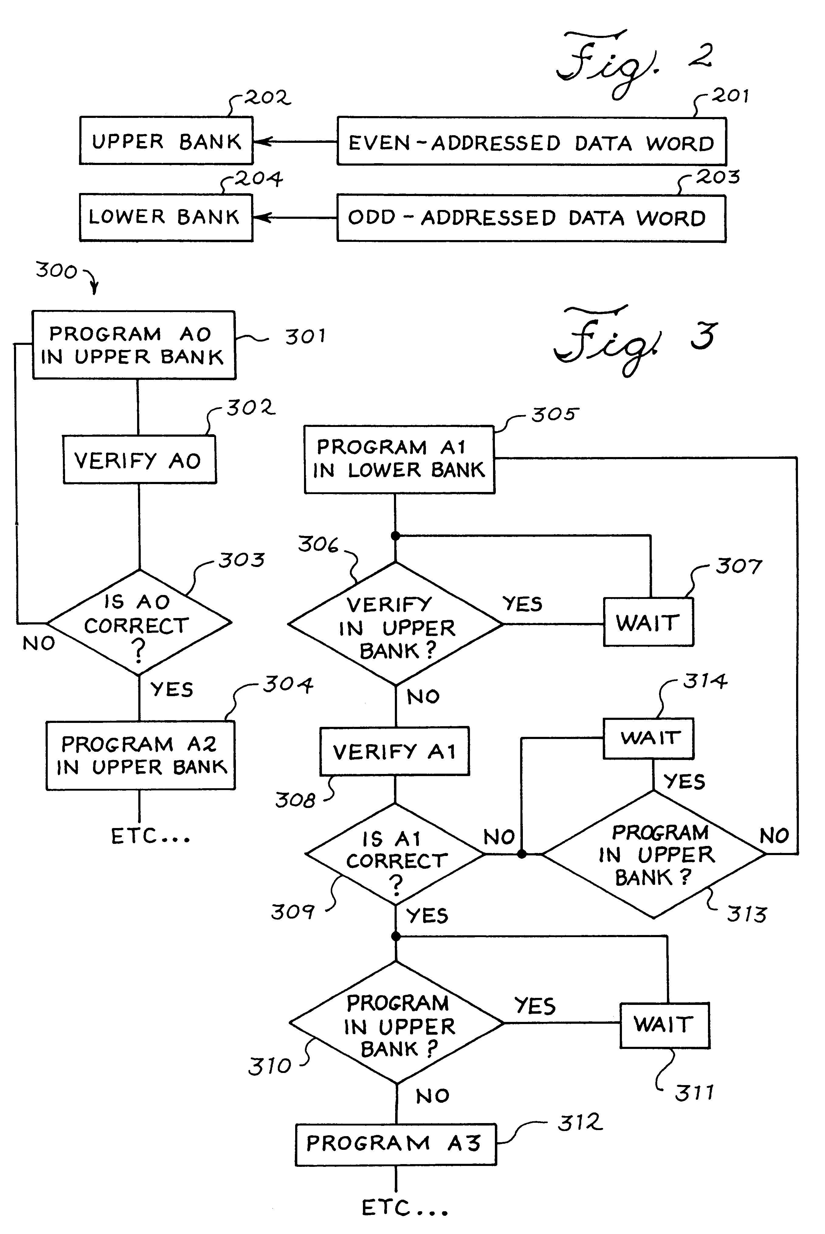
FIG. 1 illustrates a non-volatile memory device 100 that enables simultaneous program and program-verify operations according to one embodiment. Memory device 100 includes an address input (Addr) 102, a data input / output (Data) 104, power inputs (Vcc, Vss, and Vpp) 106, and control inputs 108. The control inputs 108 include Reset (RESET#), Write Enable (WE#), Chip Enable (CE#), Clock (CLK), and Output Enable (OE#). The Chip Enable signal activates the chip's control logic and input buffers (not shown). When Chip Enable is not asserted, the memory device operates in standby mode. Output Enable is used to gate the outputs of the device through I / O buffers during read cycles. Write Enable is used to enable the write functions of the memory device. In one embodiment, all of the components of FIG. 1 are contained on a single integrated circuit chip.

Memory device 100 is configured into an upper bank 110 and a lower bank 112 that are arrays (or sectors) of flash memory cells. However, othe...


PUM


Abstract

A memory device is split into two or more memory banks. Each bank includes a number of sectors. Each Sector includes memory cells. While one bank is busy with program operation, the other bank can be simultaneously engaged in program-verify operation during the same cycle.

Description

The present invention relates generally to electrically erasable and programmable non-volatile memories. More particularly, this invention relates to a method and circuit that speeds up the programming and program verification operations of a memory device by simultaneously programming in one bank and verifying the programming in another bank of a memory device.Electronic systems typically include processors and memory. The memory is used to store instructions and data. In some systems, such as cellular phones, non-volatile memory is needed to ensure that the stored data is not lost even when the system is turned off. One non-volatile memory family is Read Only Memory (ROM), Programmable ROM (PROM), and Erasable-Programmable ROM (EPROM), with varying degrees of flexibility of use. ROM memories have high density, low power consumption, and high performance, but they are not in-system updateable. On the other hand is the volatile memory family of Random Access Memory (RAM), Dynamic RA...

Claims


Application Information

Patent Timeline
IPC IPC(8): G11C16/10G11C16/06G11C16/34
CPCG11C16/10G11C16/3436G11C2216/22
Inventor AL-SHAMMA, ALI
Owner MONTEREY RES LLC
Learn More