
Process for concurrently molding semiconductor chips without void and wire weep and molding die used therein

a semiconductor chip and molding die technology, applied in the direction of semiconductor/solid-state device details, manufacturing tools, food shaping, etc., can solve the problems of high density, glass fiber reinforced epoxy resin and polyimide tape, and the area occupied by semiconductor chips is only fifty percent of the total area of the expensive panel

Inactive Publication Date: 2001-03-13
RENESAS ELECTRONICS CORP
View PDF18 Cites 30 Cited by
  • Summary
  • Abstract
  • Description
  • Claims
  • Application Information

AI Technical Summary

Problems solved by technology

For this reason, the manufacturer can not arrange the semiconductor chips on the printed circuit panel at high dense.
The glass fiber reinforced epoxy resin and the polyimide tape are expensive.
In fact, the areas occupied by the semiconductor chips are only fifty percent of the total area of the expensive panel.
The uneconomical usage of the expensive panel makes the production cost of the semiconductor device high.
On the other hand, a problem is encountered in the prior art process disclosed in Japanese Patent Publication of Unexamined Application No. 6-244313 in the scratch lines on the semiconductor wafer and voids after the molding.
If the scratch lines are deviated from the grooves, the semiconductor chips are liable to be damaged in the separation stage.
The projections are an obstacle against the melted synthetic resin flowing into the cavity, and the voids are produced in the large piece of synthetic resin due to the non-smooth flow of the melted synthetic resin.
It is difficult to use the prior art process for a large-sized package and in a concurrent molding for a large number of semiconductor chips.
Moreover, the plastic ball grid array package and the chip size package have not been standardized, yet.
The molding dies are expensive, and increase the production cost.

Method used


Image

  • Process for concurrently molding semiconductor chips without void and wire weep and molding die used therein
  • Process for concurrently molding semiconductor chips without void and wire weep and molding die used therein
  • Process for concurrently molding semiconductor chips without void and wire weep and molding die used therein

Examples


Embodiment Construction

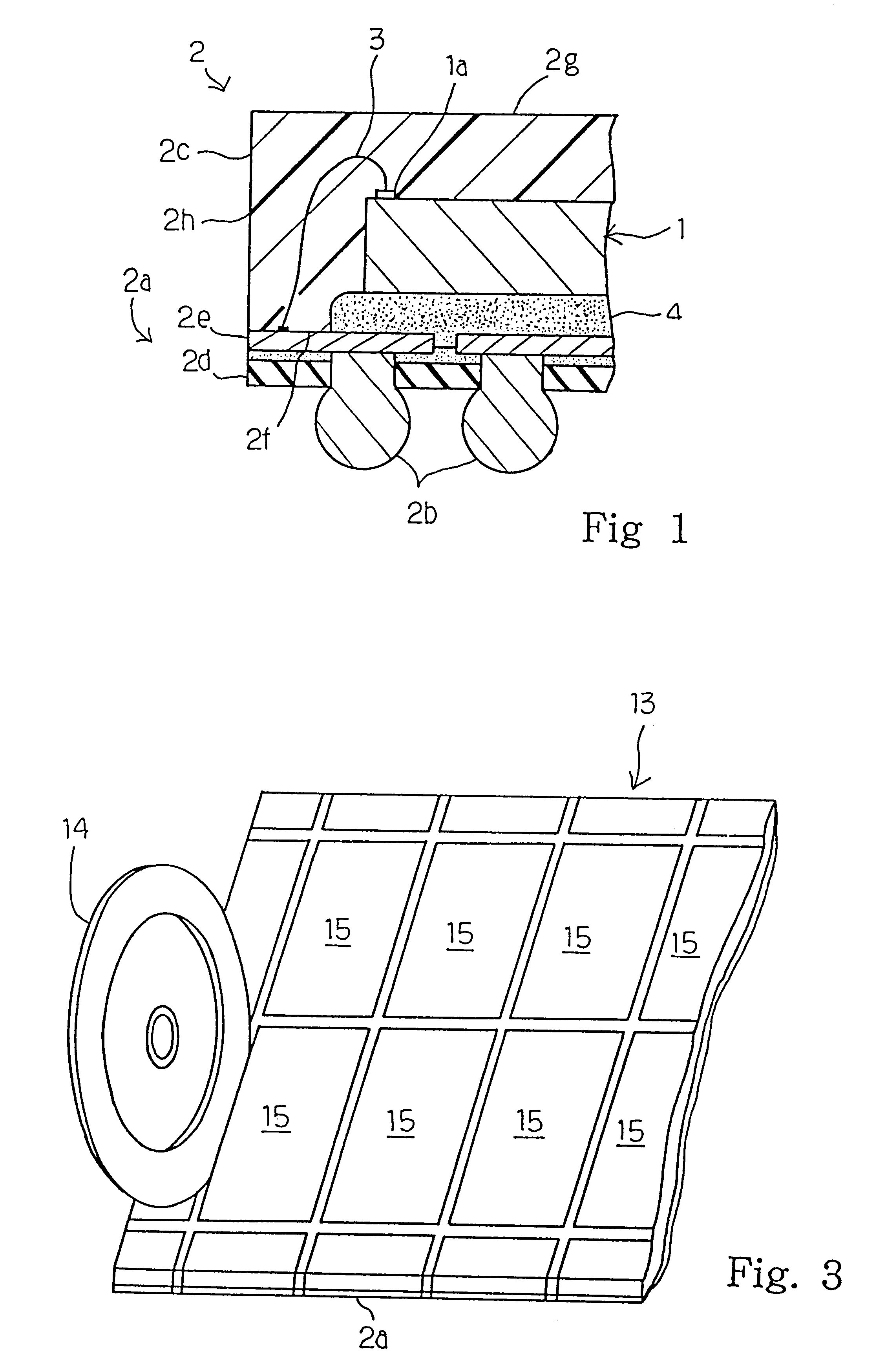
FIG. 1 illustrates a semiconductor device fabricated through a process embodying the present invention. The semiconductor device largely comprises a semiconductor chip 1, a package 2 and conductive wires 3. Though not shown in FIG. 1, circuit components and wiring lines are incorporated in the semiconductor chip 1, and form an integrated circuit. The integrated circuit is connected to bonding pads 1a, and only one bonding pad 1a is shown in figure

The package 2 is broken down into a substrate 2a, ball bumps 2b and a piece of synthetic resin 2c. The synthetic resin is dielectric, and is a kind of thermosetting resin such as, for example, a long gel type thermosetting resin. The substrate 2a includes an insulating tape 2d such as, for example, polyimide and a conductive pattern 2e of copper adhered to the insulating tape 2d. Though-holes are formed in the insulating tape 2d, and the conductive pattern 2e is exposed to the through-holes. The ball bumps 2b pass through the through-holes,...


PUM

PropertyMeasurementUnit
Lengthaaaaaaaaaa
Flow rateaaaaaaaaaa
Widthaaaaaaaaaa

Abstract

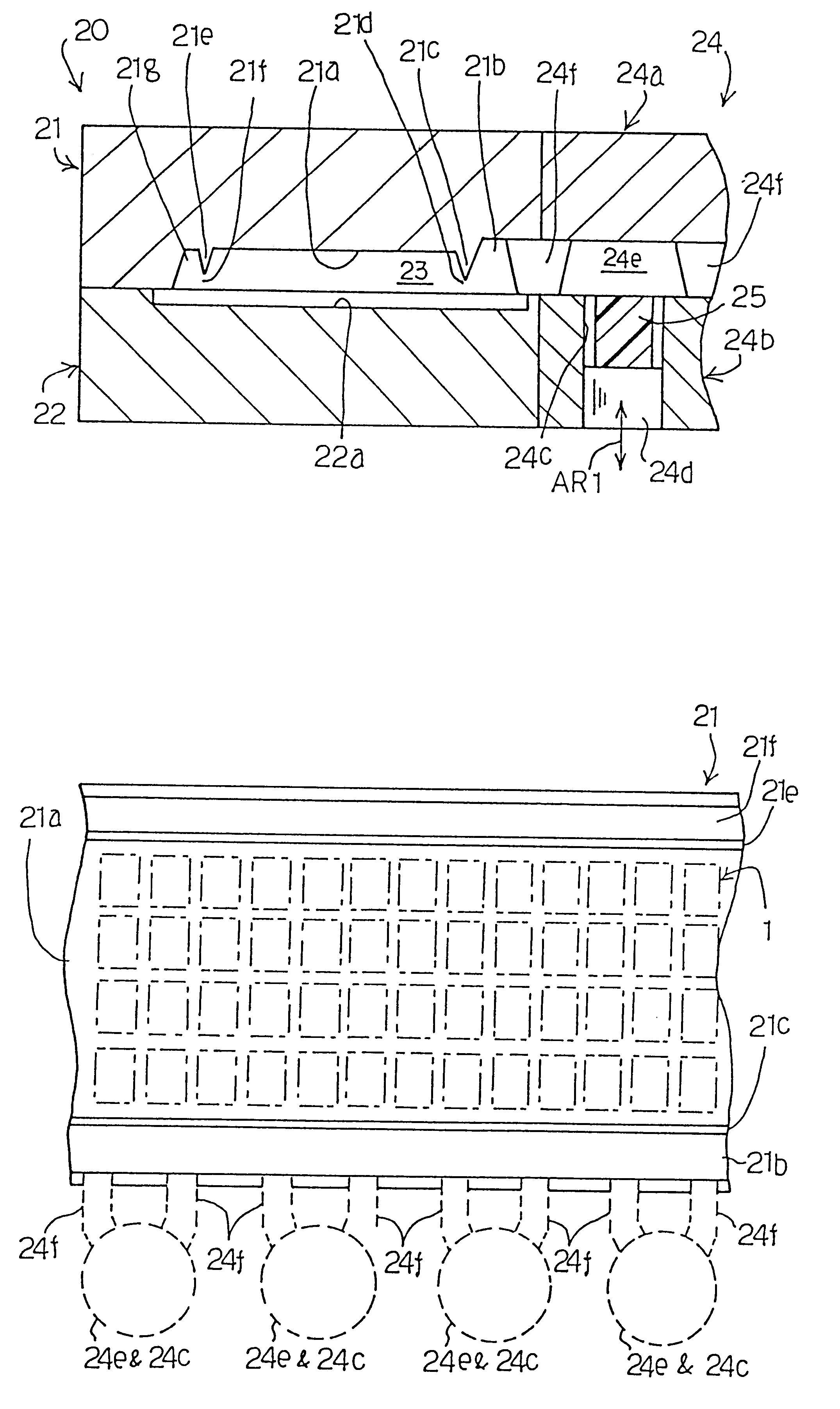
A molding die used for concurrently packaging semiconductor chips in a large piece of synthetic resin has a cavity rectangular in cross section and having two long peripheral lines and two short peripheral lines for accommodating a circuit panel where the semiconductor chips are mounted, melted synthetic resin is supplied through a gate extending along one of the long peripheral lines to the cavity so that the melted synthetic resin smoothly flows over the cavity, and the smooth flow prevents the molded product from voids and a wire weep.

Description

This invention relates to a packaging technology and, more particularly, to a process for molding semiconductor chips and a molding die used therein.DESCRIPTION OF THF RELATED ARTVarious kinds of package are used for semiconductor devices. A tape ball grid array package, a plastic ball grid array package, a fine pitch ball grid array package and a chip size package are examples of the known package. A surface-mounting package such as the plastic ball grid array package and the chip size package has a ball grid array directly connected to a circuit board, and is appropriate for miniature electric products.A typical example of the packaging process is disclosed in Japanese Patent Publication of Unexamined Application No. 9-252065. The prior art packaging process starts with preparation of a printed circuit panel. A conductive pattern was printed on an insulating plate of glass fiber reinforced epoxy resin or polyimide, and the conductive pattern and the insulating plate as a whole con...

Claims


Application Information

Patent Timeline
IPC IPC(8): B29C45/27B29C45/14B29C45/26H01L21/56H01L21/02B29C45/02B29L31/34
CPCB29C45/14655B29C45/2669B29C45/2708H01L21/565H01L24/97H01L2224/48091H01L2224/73265H01L2224/97H01L2924/01004H01L2924/01029H01L2924/01082H01L2924/14H01L2924/15184H01L2924/15311H01L2224/85H01L2924/00014H01L2224/83H01L2924/01005H01L2924/01006H01L2924/01023H01L2924/01033H01L2224/32225H01L2224/48227H01L2924/00H01L2224/32013H01L2224/73204H01L2924/181H01L2924/00012
Inventor TSURUTA, HISAYUKI
Owner RENESAS ELECTRONICS CORP
Learn More