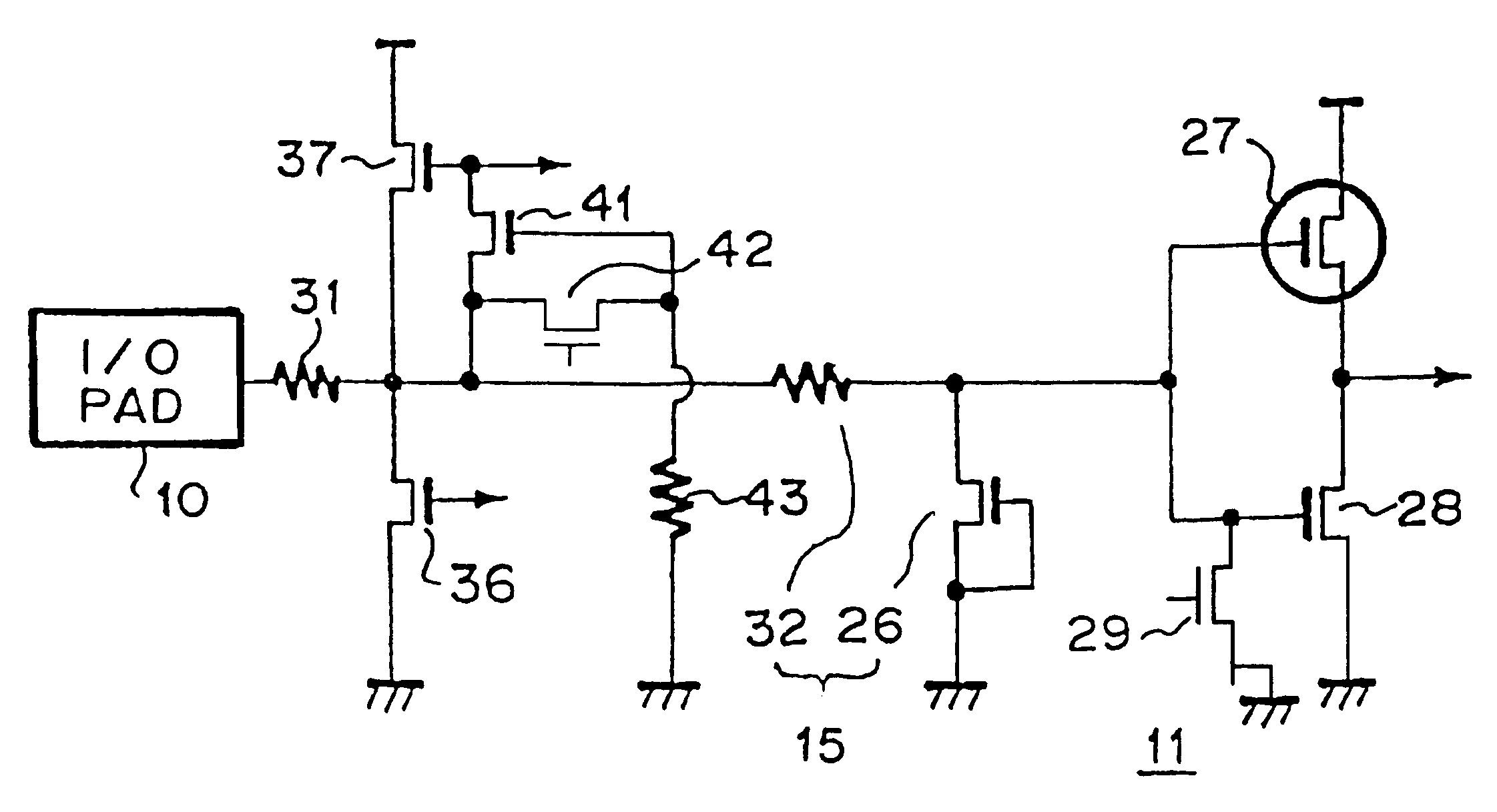

Semiconductor integrated circuit with protection circuit against electrostatic discharge

a technology of integrated circuits and shielding circuits, applied in the direction of diodes, automatic control of pulses, and semiconductor/solid-state devices, etc., can solve the problems of complex circuit construction, and inability to improve integration degr

Inactive Publication Date: 2001-02-20
LONGITUDE LICENSING LTD
View PDF15 Cites 10 Cited by
  • Summary
  • Abstract
  • Description
  • Claims
  • Application Information

AI Technical Summary

Benefits of technology

In accordance with the present invention, there is provided a parasitic bipolar transistor as a clamping element to prevent the breakdown of a semiconductor integrated circuit.

Problems solved by technology

Therefore, the conventional circuit as disclosed in the above-mentioned reference has a disadvantage that the construction of the circuit becomes complex and the integration degree can not be improved.
Further, the circuit construction becomes more complex, so as to prevent the breakdown of the protection MOSFET itself.
The fact is that the breakdown could not be prevented even by inserting any protection element between the input pad and the ground.

Method used


Image

  • Semiconductor integrated circuit with protection circuit against electrostatic discharge
  • Semiconductor integrated circuit with protection circuit against electrostatic discharge

Examples


Embodiment Construction

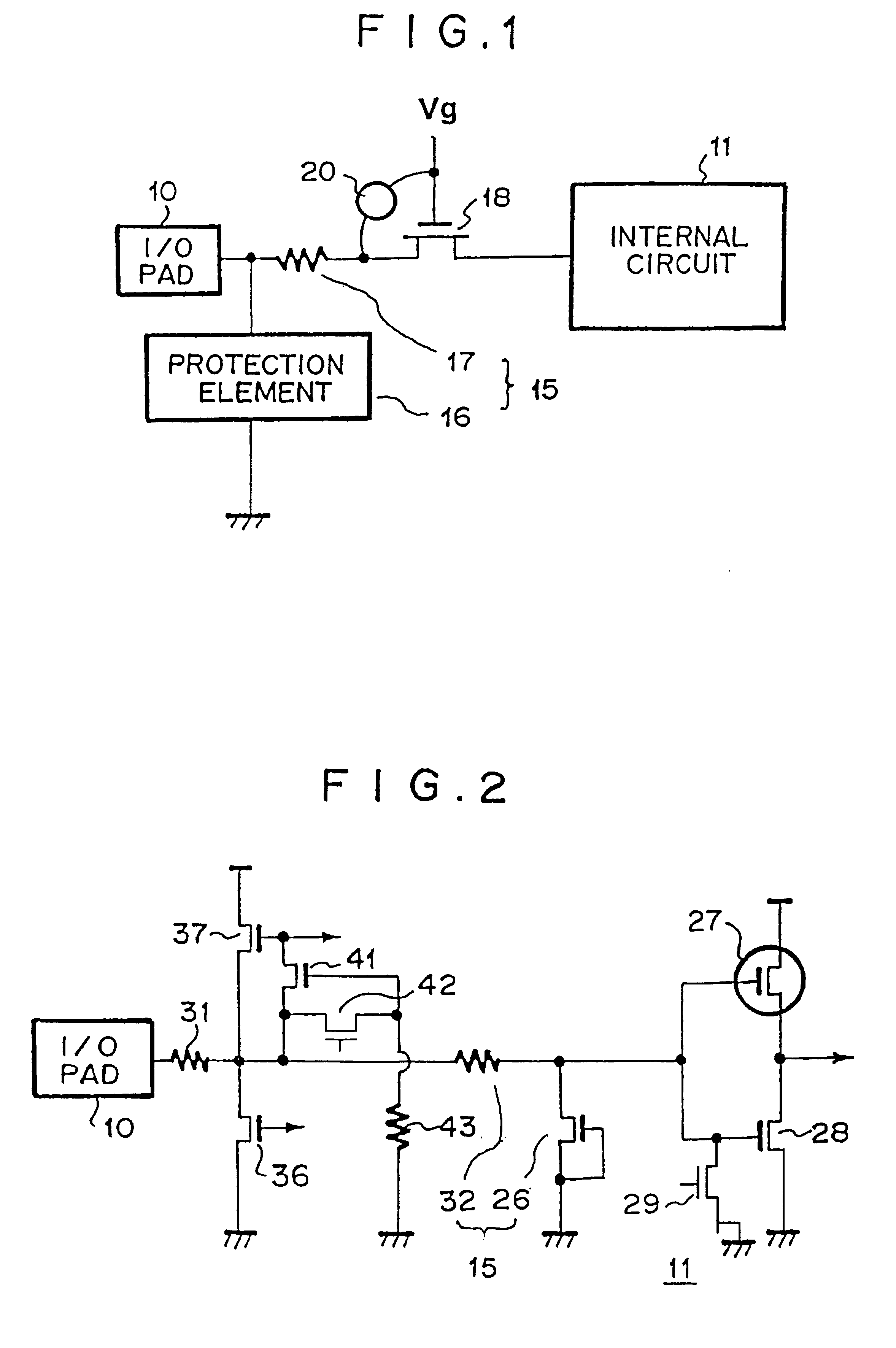
Referring to the drawings, a preferred embodiment of the present invention is explained.

A semiconductor integrated circuit of the present invention as shown in FIG. 1 comprises input pad 10 and internal circuit 11. Further, transfer gate 18 comprising a MIS transistor is connected between input pad 10 and internal circuit 11. Here, input pad 10 may be replaced by an output pad.

Concretely, protection circuit 15 comprises protection element 16 such as diode, and resistor 17. The gate of MIS transistor 18 is supplied with voltage Vg by an internal voltage source or an external voltage source.

Further, clamping element 20 is connected between the gate and either of the source or the drain of MIS transistor 18. Clamping element 20 is adjacent to MIS transistor 18.

Here, the behavior of protection circuit is explained, assuming that clamping element is not inserted. In this case, the electrostatic voltage applied to input pad 10 in the human body model is clamped by protection element 16. T...


PUM


Abstract

A Semiconductor integrated circuit with a protection circuit against electrostatic discharge. A clamping element is connected with MIS transistor to prevent the breakdown under the charged device model. A parasitic bipolar transistor, a MOS transistor or MIS transistor whose gate is composed of an insulating film thicker than that of the transfer gate, can be used as the clamping element.

Description

1. Technical Field of the InventionThe present invention relates to a semiconductor integrated circuit which may possibly be destroyed by electrostatic discharge and particularly, to a semiconductor integrated circuit provided with metal insulator semiconductor (MIS) transistor as a transfer gate.2. Description of the Prior ArtGenerally, the breakdown of semiconductor integrated circuits by electrostatic discharge is of great interest, as the scale of integrated circuits becomes greater. Consequently, various models such as human model, charged device model and charged package model are used to analyze the electrostatic breakdown of integrated circuits. It is desirable that the integrated circuits do not suffer the electrostatic breakdown under each model. Particularly, the integrated circuit is usually required to be resistant electrostatically against around 600 Volt under the charged device model and the charged package model.For preventing the electrostatic discharge, there is d...

Claims


Application Information

Patent Timeline
Patent Type & Authority Patents(United States)
IPC IPC(8): H01L27/02H03K5/08
CPCH01L27/0251H01L27/0255H01L27/0288H03K5/08H01L2924/0002H01L2924/00H01L23/60
Inventor FUJII, TAKEONARITA, KAORUHORIGUCHI, YOKO
Owner LONGITUDE LICENSING LTD
Learn More