High precision three-dimensional alignment system for lithography, fabrication and inspection

a three-dimensional alignment and lithography technology, applied in the direction of instruments, electrical controllers, program control, etc., can solve the problems of limiting the prompt application of such photolithography systems, affecting the participation of the participants, and affecting the quality of the finished produ

Inactive Publication Date: 2001-01-30
INST OF MATERIALS RES & ENG
View PDF3 Cites 9 Cited by
  • Summary
  • Abstract
  • Description
  • Claims
  • Application Information

AI Technical Summary

Benefits of technology

It is another object of the present invention to reduce the requirement for complex scribing tool designs in nanolithography.
It is a further object of the present invention to provide an SPM system which allows for multi-probe imaging of surfaces.

Problems solved by technology

The lack of efficient light source past the ArF laser line at 193 nm and the unavailability of good optical materials may limit prompt application of such photolithography systems.
Although other techniques like the e-beam and X-ray lithography may serve as attractive alternatives, precise optimization of process parameters and technical-related issues may further hinder their participation.
Although this photolithography method allows a plurality of cantilevers to operate within the same photolithographic wafer, there are the following limitations to the method.
Firstly, the fabrication of the cantilevers and waveguides is a complex process and therefore expensive.
In addition, due to the complex fabrication process, the resulting cantilevers and tips within the same wafer are often not uniform, resulting in difficulties in obtaining uniform alignment of tip heights.
However, this means that numerous electrical connections and capacitive plates have to be provided along the surface of the photolithographic wafer.
This not only makes the circuitry extremely complex, but also limits the number of cantilevers which can be realistically controlled within one photolithographic wafer.
Secondly, if a cantilever has to be flexed to a relatively large degree before the desired gap distance can be reached, the tip may be positioned to face the fabrication wafer at an angle substantially different from normal.
It is clear that although alignment obtained using this method is in the order of a few nanometers, this method only allows two dimensional alignment.
When a third dimension of alignment is required, such as for multiple tip scribing wafers, this method would not be useful for preventing tilting of scribing tools.

Method used


Image

  • High precision three-dimensional alignment system for lithography, fabrication and inspection
  • High precision three-dimensional alignment system for lithography, fabrication and inspection
  • High precision three-dimensional alignment system for lithography, fabrication and inspection

Examples


Embodiment Construction

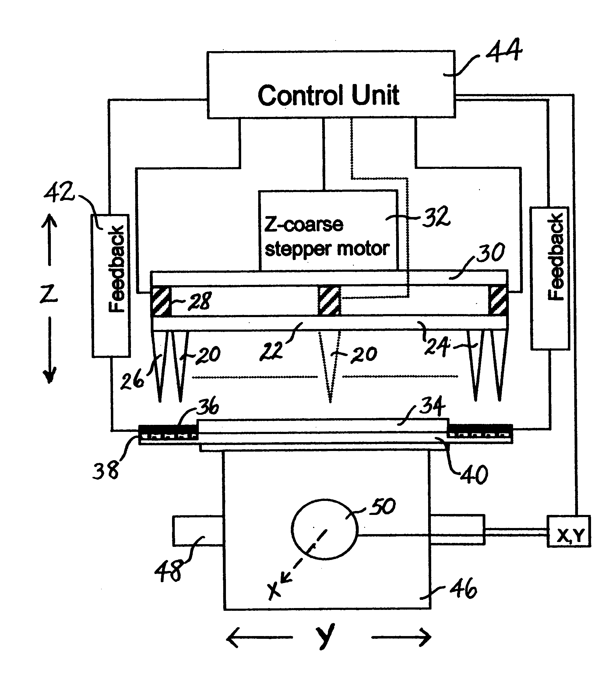
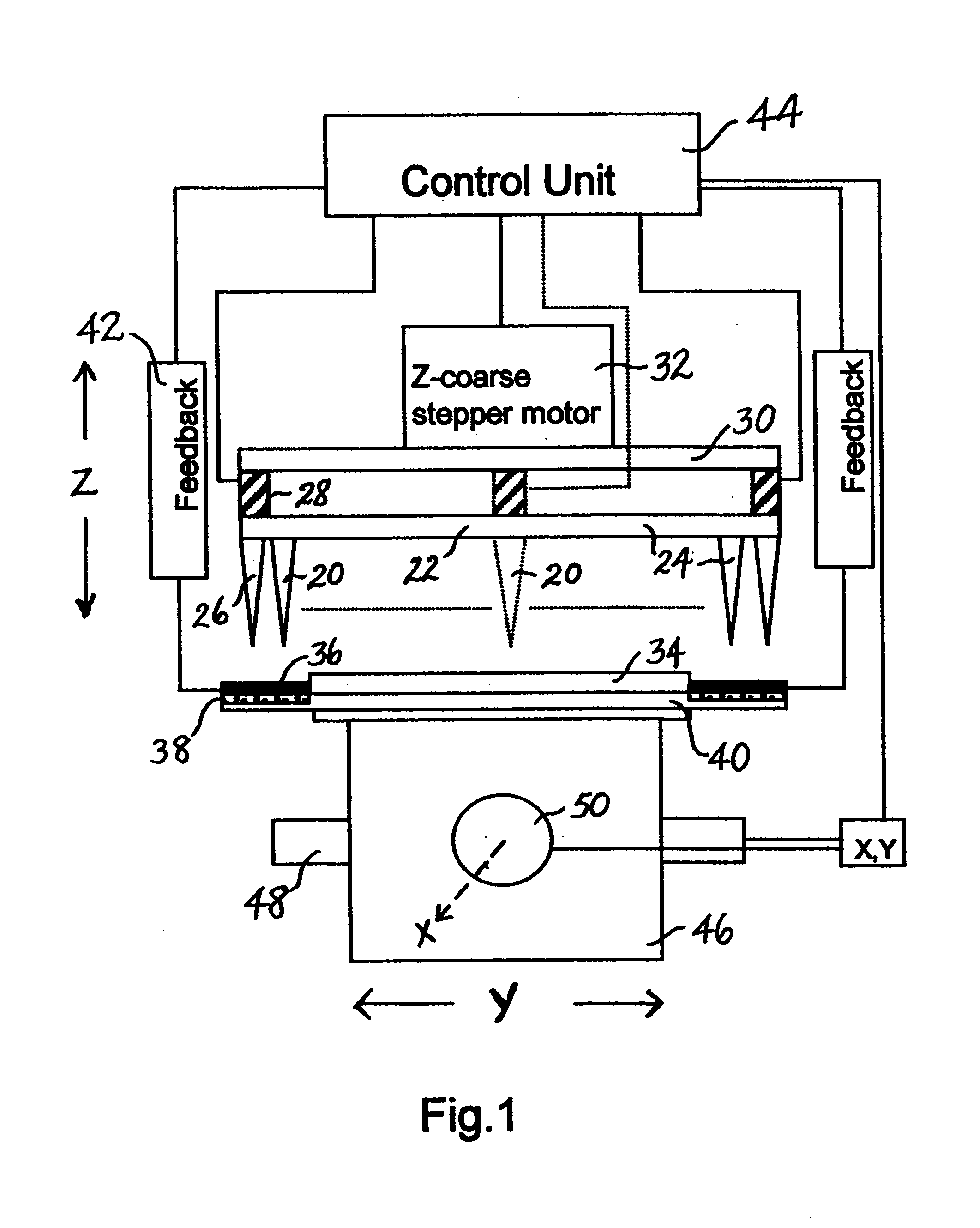
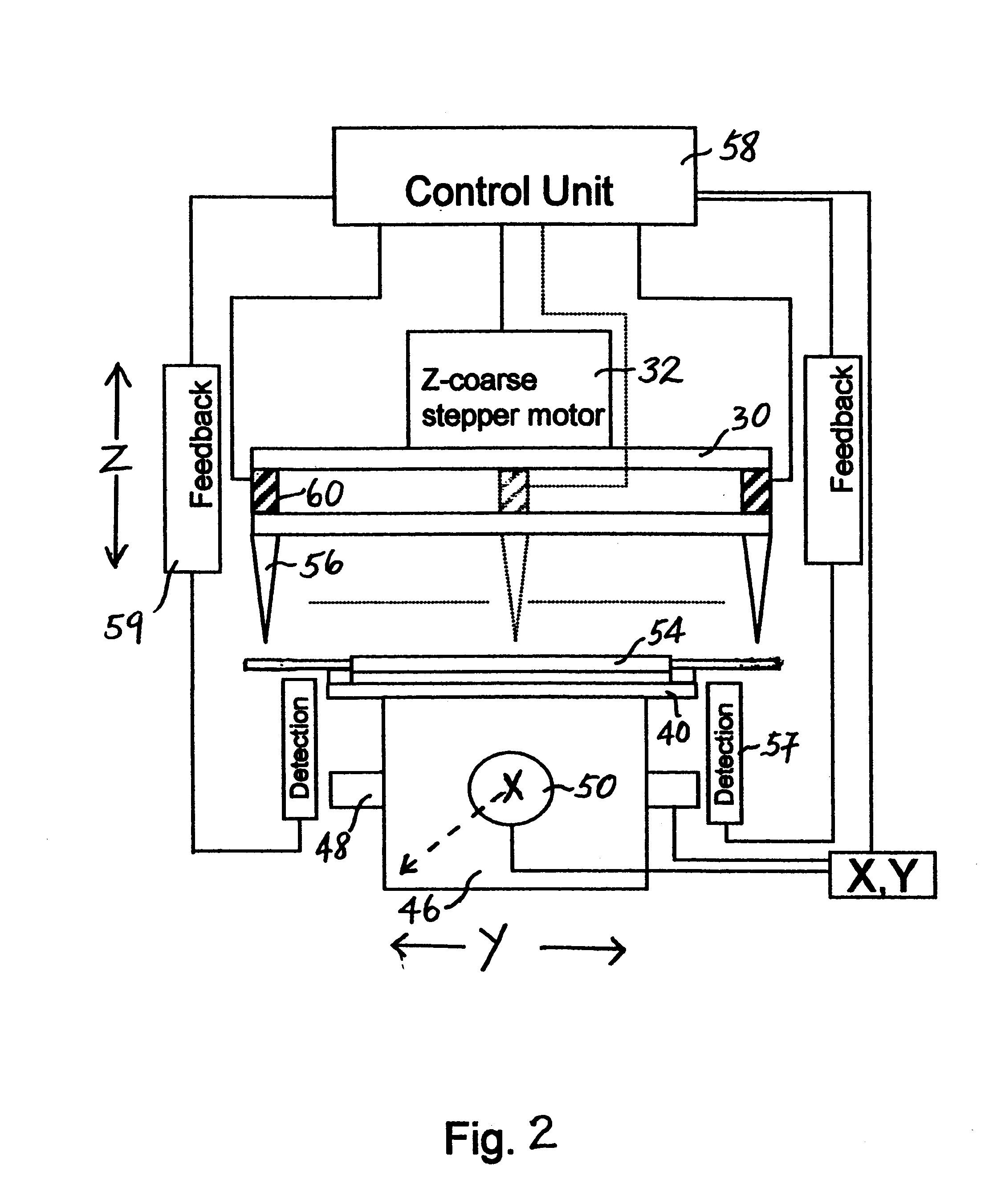
The present invention uses scanning probe microscopy techniques to provide a high precision three-dimensional microalignment system. Microalignment and micromanipulation refer to alignment and manipulation on a micrometer, nanometer or subnanometer scale. The features of this system is described below using nanolithography as an example. The nanolithography features and images produced may be as small as subnanometers to hundreds of nanometers. Two embodiments of the present invention will be described. In both embodiments, piezoelectric material is provided for the fine distance control unit. The first embodiment provides a piezoelectric sensor to sense the approach of the scribing tips. The second embodiment provides other types of proximity detectors for the same purpose.

Referring to FIG. 1, this embodiment of the present invention comprises a plurality of tips 20 fabricated on the base 22 of a scribing tool 24 such as a silicon wafer to perform fabrication of sub-100 nm features...


PUM


Abstract

The present invention provides a high precision three-dimensional alignment system using SPM techniques and method of using the same. The system comprises a fine distance control unit for the effective three-dimensional micromovement in the nanometer range of a planar object, and proximity detection unit to monitor the alignment process. In the preferred embodiment, the fine distance control unit comprises a set of at least three strategically positioned fine distance control elements which are capable of controlled expansion and contraction in the nanometer range. The most preferred embodiment of the fine distance control element comprises a piezoelectric tube, which crystal size may be varied by varying an applied voltage. This system may be applied to microlithography, in which case the planar object is a scribing tool having a planar base with multiple tips fabricated on one surface.

Description

The present invention is related to a high precision three-dimensional alignment systems using scanning probe microscopy (SPM) techniques. In particular, the present invention is related to a three-dimensional alignment system for lithography and fabrication. The present invention also relates to a high precision alignment system for SPM inspection.Since the advent of scanning tunneling microscopy and atomic force microscopy, intensive research interest in the field of nanometer and submicrometer length scale surface modifications utilizing the above-mentioned techniques has been expressed. These fabrications usually involve controlled modifications of the surface morphologies which are critical and important for the fabrication of miniaturized micromechanical and electronic devices with nanometer scale dimensions. It becomes more significant when one considers the limitations encountered by the photolithography systems as device dimensions are constantly being scaled down to the su...

Claims


Application Information

Patent Timeline
IPC IPC(8): G05B19/402
CPCG05B19/402B82Y10/00G05B2219/37404G05B2219/45028G05B2219/50379G11B9/14Y10S977/851Y10S977/856
Inventor LI, SAM FONG YAUNG, HOU TEE
Owner INST OF MATERIALS RES & ENG
Why Eureka
Try Eureka