
Substrate inspection method and apparatus

Inactive Publication Date: 2001-01-23
APPLIED MATERIALS INC
View PDF20 Cites 186 Cited by
  • Summary
  • Abstract
  • Description
  • Claims
  • Application Information

AI Technical Summary

Benefits of technology

In particular, an object of the invention is to provide a method and apparatus for automatically inspecting patterned semiconductor wafers characterized by a relatively high speed and relatively low rate of false alarms such that the patterned wafers may be tested while the wafers are in the production line to quickly enable the fabrication personnel to identify any process or equipment causing yield reduction, to receive fast feedback information after corrective actions, and to predict potential yield loss.
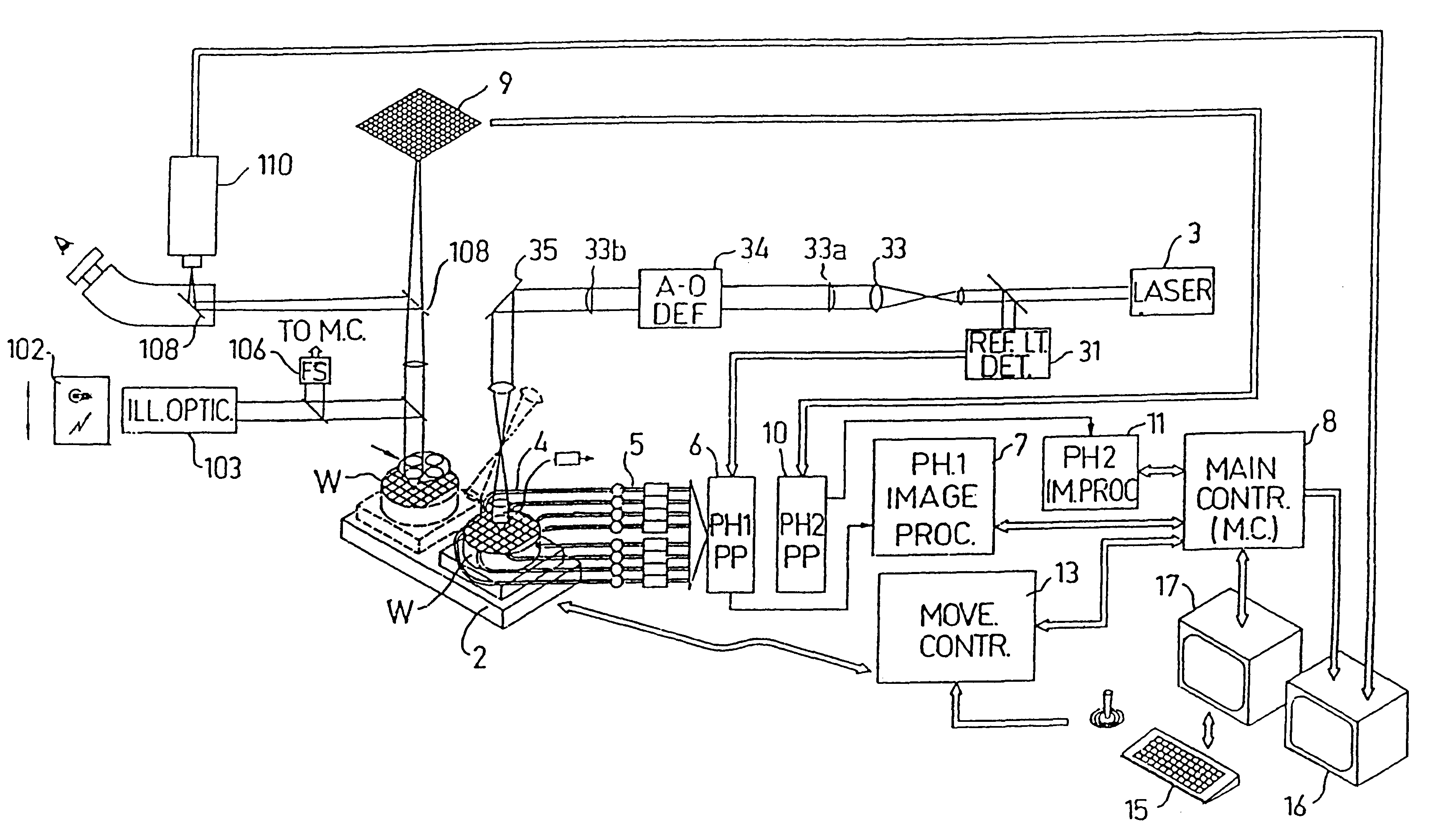
It will thus be seen that the novel method of the present invention primarily monitors changes in the defect density while maintaining a high throughput with a relatively low false alarm rate. Thus, the first examination is done at a relatively high speed and with a relatively low spatial resolution such as with a laser beam of small diameter to indicate only suspected locations having a high probability of a defect; and the second examination is done with a relatively high spatial resolution but only with respect to the suspected locations having a high probability of a defect. The sensitivity of the two phases may be adjusted according to the requirements for any particular application. Thus, where the application involves a relatively low number of defects, the sensitivity of the first examination phase may be increased by using a very small diameter laser beam to detect very small defects at a high speed but at the expense of an increased false alarm rate. However, since only relatively few suspected locations are examined in the second phase, the overall inspection can be effected relatively quickly to enable the fabrication personnel to identify defects caused by any process or equipment, and to immediately correct the cause for such defects.

Problems solved by technology

However, the inspection of patterned semiconductor wafers for defects in the pattern is considerably more difficult because the light scattered by the pattern overwhelms the light scattered from the particles or defects, thereby producing high rates of false alarms.
However, the extremely large number of pixels involved makes such systems extremely slow.
As a result, microdefects in patterned semiconductor wafers remain largely undetected until a considerable number of such wafers have been fabricated and have begun to exhibit problems caused by the defects.
The late discovery of such defects can therefore result in considerable losses, low yields, and large downtimes.

Method used


Image

  • Substrate inspection method and apparatus
  • Substrate inspection method and apparatus
  • Substrate inspection method and apparatus

Examples


Embodiment Construction

Overall System

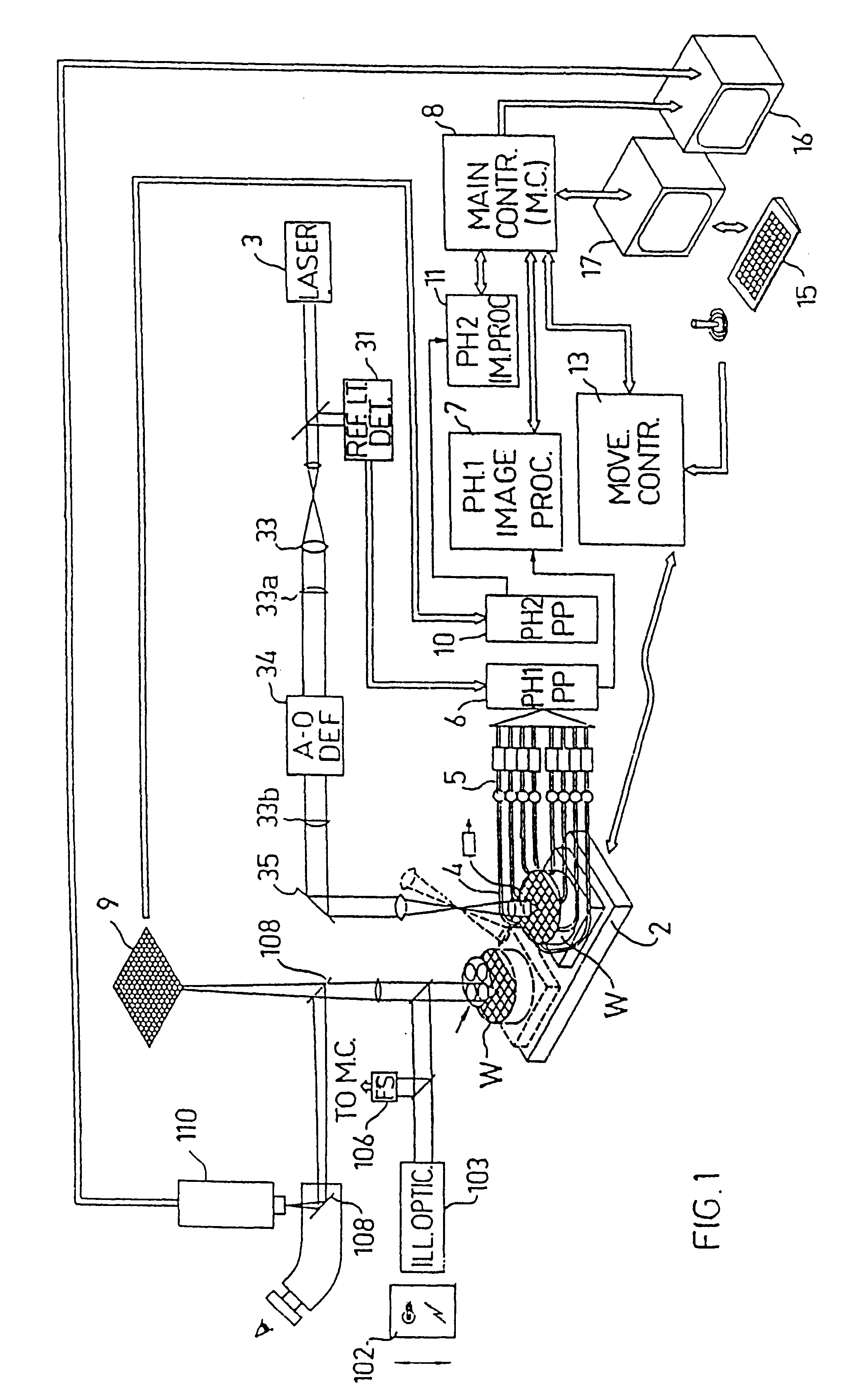
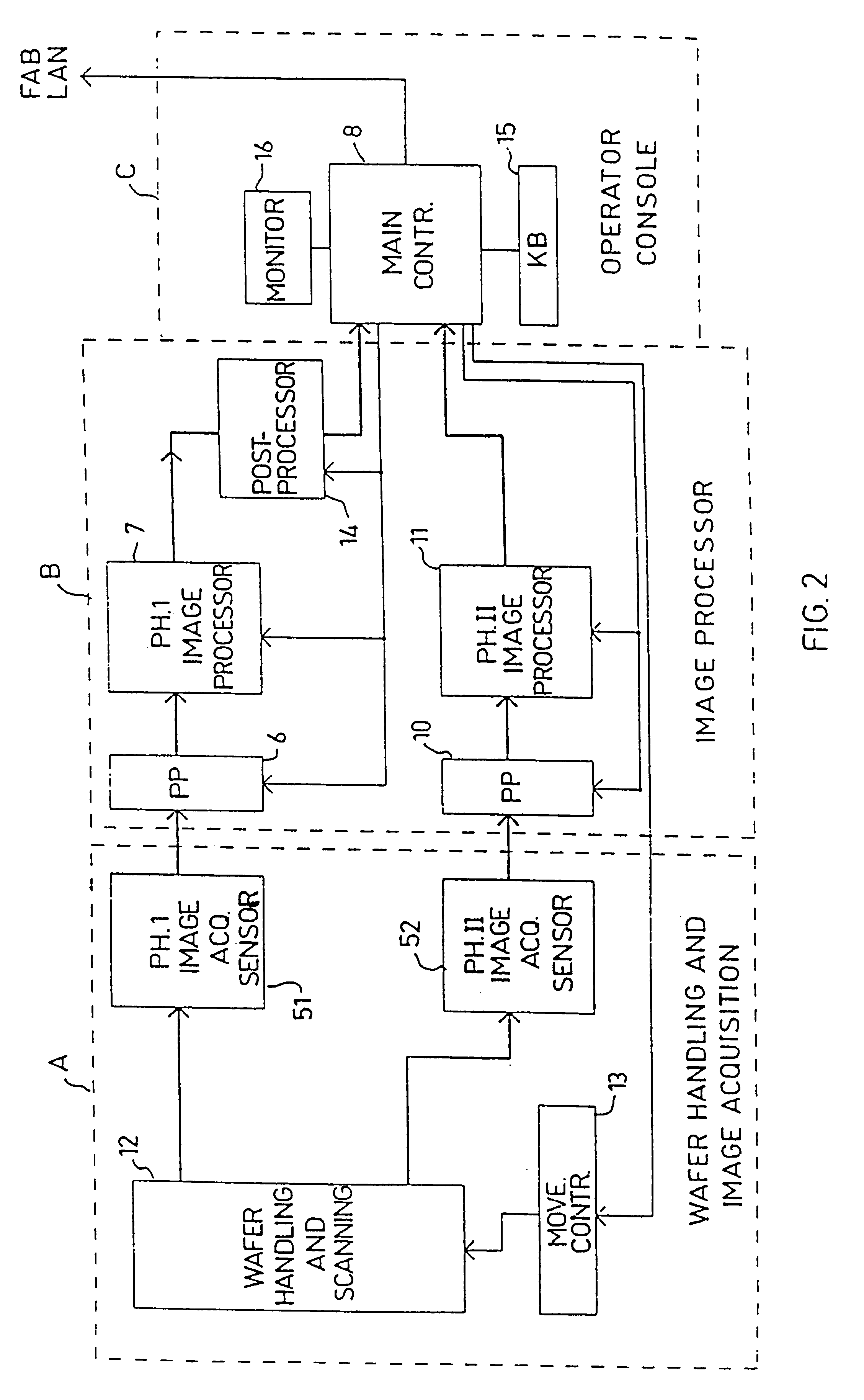
The system illustrated in the drawings is designed particularly for automatically inspecting patterned semiconductor wafers having a plurality of like integrated-circuit dies each formed with like patterns. The system inspects each pattern, called the inspected pattern, by comparing it with at least one other pattern on the wafer, serving as the reference pattern, to detect any differences which would indicate a defect in the inspected pattern.

The inspection is made in two phases: In the first phase, the complete surface of the wafer is inspected at a relatively high speed and with a relatively low spatial resolution; and information is outputted indicating suspected locations on the wafer having a high probability of a defect. These locations are stored in a storage device. In the second phase, only the suspected locations stored in the storage device are examined with a relatively high spatial resolution; and a determination is made as to the presence or absence of a...


PUM


Abstract

A method and apparatus for inspecting the surface of articles, such as chips and wafers, for defects, includes a first phase of optically examining the complete surface of the article inspected at a relatively high speed and with a relatively low spatial resolution, and a second phase of optically examining with a relatively high spatial resolution only the suspected locations for the presence or absence of a defect therein.

Description

FILED AND BACKGROUND OF THE INVENTIONThe present invention relates to a method and apparatus for optically inspecting the surface of an article for defects. The invention is particularly useful for optically inspecting patterned semiconductor wafers used in producing integrated-circuit dies or chips, and the invention is therefore described below particularly with respect to this application.The inspection of unpatterned semiconductor wafers for surface-lying particles is relatively simple and can be easily automated. In one known type of such system, the wafer is scanned by a laser beam, and a photodetector detects the presence of a particle by collecting the light scattered by the particle. However, the inspection of patterned semiconductor wafers for defects in the pattern is considerably more difficult because the light scattered by the pattern overwhelms the light scattered from the particles or defects, thereby producing high rates of false alarms.The existing inspection syste...

Claims


Application Information

Patent Timeline
IPC IPC(8): G01N21/956G01N21/88G01N21/94G01N21/95
CPCG01N21/94G01N21/9501G01N21/956G01N2021/8822G01N2021/8825G01N2021/8854G01N2021/8861G01N2021/8864G01N2021/8867G01N2021/887
Inventor ALUMOT, DAVIDNEUMANN, GADSHERMAN, RIVKATIROSH, EHUD
Owner APPLIED MATERIALS INC
Learn More